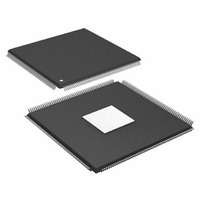
ADSP-21371KSWZ-2B Analog Devices Inc, ADSP-21371KSWZ-2B Datasheet - Page 44

ADSP-21371KSWZ-2B
Manufacturer Part Number
ADSP-21371KSWZ-2B
Description
IC DSP 32BIT 266MHZ 208-LQFP
Manufacturer
Analog Devices Inc
Series
SHARC®r
Type
Floating Pointr
Specifications of ADSP-21371KSWZ-2B
Package / Case
208-LQFP
Interface
DAI, DPI
Operating Temperature
0°C ~ 70°C
Clock Rate
266MHz
Non-volatile Memory
ROM (512 kB)
On-chip Ram
128kB
Voltage - I/o
3.30V
Voltage - Core
1.20V
Mounting Type
Surface Mount
Svhc
No SVHC (18-Jun-2010)
Base Number
21371
Core Frequency Typ
266MHz
Dsp Type
Floating Point
Mmac
532
No. Of Pins
208
Interface Type
SPI, UART
Rohs Compliant
Yes
Operating Temperature Range
0°C To +70°C
Lead Free Status / RoHS Status
Lead free / RoHS Compliant
Available stocks
Company
Part Number
Manufacturer
Quantity
Price
Company:
Part Number:
ADSP-21371KSWZ-2B
Manufacturer:
Analog Devices Inc
Quantity:
10 000
Part Number:
ADSP-21371KSWZ-2B
Manufacturer:
ADI/亚德诺
Quantity:
20 000
ADSP-21371
OUTPUT DRIVE CURRENTS
Figure 34
ers of the ADSP-21371. The curves represent the current drive
capability of the output drivers as a function of output voltage.
TEST CONDITIONS
The ac signal specifications (timing parameters) appear in
Table 15 on Page 21
output disable time, output enable time, and capacitive loading.
The timing specifications for the SHARC apply for the voltage
reference levels in
Timing is measured on signals when they cross the 1.5 V level as
described in
sured between the point that the first signal reaches 1.5 V and
the point that the second signal reaches 1.5 V.
- 20
- 30
- 40
- 10
40
30
20
10
Figure 34. ADSP-21371 Typical Drive at Junction Temperature
OUTPUT
0
Figure 35. Equivalent Device Loading for AC Measurements
0
OUTPUT
Figure 36. Voltage Reference Levels for AC Measurements
PIN
TO
INPUT
shows typical I-V characteristics for the output driv
OR
V
Figure
OL
0.5
1.5V
Figure
3.47V, 45°C
36. All delays (in nanoseconds) are mea
SWEEP (V
through
1.0
(Includes All Fixtures)
35.
3.11V, 125°C
1.5
DDEXT
Table 41 on Page
30pF
) VOLTAGE (V)
2.0
V
OH
3.11V, 125°C
50�
2.5
3.3V, 25°C
43. These include
3.0
3.3V, 25°C
Rev. 0 | Page 44 of 48 |
3.47V, -45°C
1.5V
3.5
1.5V
CAPACITIVE LOADING
Output delays and holds are based on standard capacitive loads:
30 pF on all pins (see
how output delays and holds vary with load capacitance. The
graphs of
outside the ranges shown for Typical Output Delay vs. Load
Capacitance and Typical Output Rise Time (20% to 80%,
V = Min) vs. Load Capacitance.
June 2007
12
10
0
12
10
8
6
4
2
Figure
Figure 37. Typical Output Rise/Fall Time (20% to 80%,
Figure 38. Typical Output Rise/Fall Time (20% to 80%,
8
4
6
2
0
0
0
37,
y = 0.0467x + 1.6323
50
Figure
y = 0.049x + 1.5105
50
Figure
LOAD CAPACITANCE (pF)
V
LOAD CAPACITANCE (pF)
V
38, and
DDEXT
DDEXT
35).
100
100
y = 0.045x + 1.524
y = 0.0482x + 1.4604
= Max)
= Min)
Figure 39
Figure 39
RIS
150
150
RISE
E
shows graphically
FALL
FALL
may not be linear
200
200
250
250


