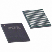
EPM2210F324C4 Altera, EPM2210F324C4 Datasheet - Page 48
EPM2210F324C4
Manufacturer Part Number
EPM2210F324C4
Description
IC MAX II CPLD 2210 LE 324-FBGA
Manufacturer
Altera
Series
MAX® IIr
Specifications of EPM2210F324C4
Programmable Type
In System Programmable
Delay Time Tpd(1) Max
7.0ns
Voltage Supply - Internal
2.5V, 3.3V
Number Of Logic Elements/blocks
2210
Number Of Macrocells
1700
Number Of I /o
272
Operating Temperature
0°C ~ 85°C
Mounting Type
Surface Mount
Package / Case
324-FBGA
Voltage
2.5V, 3.3V
Memory Type
FLASH
Number Of Logic Elements/cells
2210
For Use With
P0305 - KIT MAX II MICRO
Lead Free Status / RoHS Status
Contains lead / RoHS non-compliant
Features
-
Other names
544-1343
EPM2210F324C4
EPM2210F324C4
Available stocks
Company
Part Number
Manufacturer
Quantity
Price

Company:
Part Number:
EPM2210F324C4N
Manufacturer:
ALTERA
Quantity:
1 164
Part Number:
EPM2210F324C4N
Manufacturer:
ALTERA/阿尔特拉
Quantity:
20 000


3–6
Table 3–4. MAX II Device Family Programming Times
UFM Programming
In-System Programming Clamp
MAX II Device Handbook
Erase + Program (1 MHz)
Erase + Program (10 MHz)
Verify (1 MHz)
Verify (10 MHz)
Complete Program Cycle (1 MHz)
Complete Program Cycle (10 MHz)
f
f
Description
Table 3–4
execute the algorithm vectors in hardware. Software-based programming tools used
with download cables are slightly slower because of data processing and transfer
limitations.
The Quartus II software, with the use of POF, Jam, or JBC files, supports
programming of the user flash memory (UFM) block independent of the logic array
design pattern stored in the CFM block. This allows updating or reading UFM
contents through ISP without altering the current logic array design, or vice versa. By
default, these programming files and methods will program the entire flash memory
contents, which includes the CFM block and UFM contents. The stand-alone
embedded Jam STAPL player and Jam Byte-Code Player provides action commands
for programming or reading the entire flash memory (UFM and CFM together) or
each independently.
For more information, refer to the
chapter in the MAX II Device Handbook.
By default, the IEEE 1532 instruction used for entering ISP automatically tri-states all
I/O pins with weak pull-up resistors for the duration of the ISP sequence. However,
some systems may require certain pins on MAX II devices to maintain a specific DC
logic level during an in-field update. For these systems, an optional in-system
programming clamp instruction exists in MAX II circuitry to control I/O behavior
during the ISP sequence. The in-system programming clamp instruction enables the
device to sample and sustain the value on an output pin (an input pin would remain
tri-stated if sampled) or to explicitly set a logic high, logic low, or tri-state value on
any pin. Setting these options is controlled on an individual pin basis using the
Quartus II software.
For more information, refer to the
chapter in the MAX II Device Handbook.
shows the programming times for MAX II devices using in-circuit testers to
EPM240G
EPM240Z
EPM240
1.72
1.65
0.09
0.01
1.81
1.66
EPM570G
EPM570Z
EPM570
2.16
1.99
0.17
0.02
2.33
2.01
Using Jam STAPL for ISP via an Embedded Processor
Real-Time ISP and ISP Clamp for MAX II Devices
EPM1270G
EPM1270
2.90
2.58
0.30
0.03
3.20
2.61
Chapter 3: JTAG and In-System Programmability
EPM2210G
EPM2210
3.92
3.40
0.49
0.05
4.41
3.45
© October 2008 Altera Corporation
In System Programmability
Unit
sec
sec
sec
sec
sec
sec
Related parts for EPM2210F324C4
Image
Part Number
Description
Manufacturer
Datasheet
Request
R

Part Number:
Description:
(EPMxxxx) JTAG & In-System Programmability
Manufacturer:
Altera Corporation
Datasheet:

Part Number:
Description:
CYCLONE II STARTER KIT EP2C20N
Manufacturer:
Altera
Datasheet:

Part Number:
Description:
CPLD, EP610 Family, ECMOS Process, 300 Gates, 16 Macro Cells, 16 Reg., 16 User I/Os, 5V Supply, 35 Speed Grade, 24DIP
Manufacturer:
Altera Corporation
Datasheet:
Part Number:
Description:
CPLD, EP610 Family, ECMOS Process, 300 Gates, 16 Macro Cells, 16 Reg., 16 User I/Os, 5V Supply, 15 Speed Grade, 24DIP
Manufacturer:
Altera Corporation
Datasheet:
Part Number:
Description:
Manufacturer:
Altera Corporation
Datasheet:
Part Number:
Description:
CPLD, EP610 Family, ECMOS Process, 300 Gates, 16 Macro Cells, 16 Reg., 16 User I/Os, 5V Supply, 30 Speed Grade, 24DIP
Manufacturer:
Altera Corporation
Datasheet:
Part Number:
Description:
High-performance, low-power erasable programmable logic devices with 8 macrocells, 10ns
Manufacturer:
Altera Corporation
Datasheet:
Part Number:
Description:
High-performance, low-power erasable programmable logic devices with 8 macrocells, 7ns
Manufacturer:
Altera Corporation
Datasheet:
Part Number:
Description:
Classic EPLD
Manufacturer:
Altera Corporation
Datasheet:
Part Number:
Description:
High-performance, low-power erasable programmable logic devices with 8 macrocells, 10ns
Manufacturer:
Altera Corporation
Datasheet:
Part Number:
Description:
Manufacturer:
Altera Corporation
Datasheet:
Part Number:
Description:
Manufacturer:
Altera Corporation
Datasheet:
Part Number:
Description:
Manufacturer:
Altera Corporation
Datasheet: