EPM2210F324C4 Altera, EPM2210F324C4 Datasheet - Page 45
EPM2210F324C4
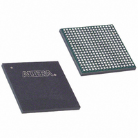
Manufacturer Part Number
EPM2210F324C4
Description
IC MAX II CPLD 2210 LE 324-FBGA
Manufacturer
Altera
Series
MAX® IIr
Specifications of EPM2210F324C4
Programmable Type
In System Programmable
Delay Time Tpd(1) Max
7.0ns
Voltage Supply - Internal
2.5V, 3.3V
Number Of Logic Elements/blocks
2210
Number Of Macrocells
1700
Number Of I /o
272
Operating Temperature
0°C ~ 85°C
Mounting Type
Surface Mount
Package / Case
324-FBGA
Voltage
2.5V, 3.3V
Memory Type
FLASH
Number Of Logic Elements/cells
2210
For Use With
P0305 - KIT MAX II MICRO
Lead Free Status / RoHS Status
Contains lead / RoHS non-compliant
Features
-
Other names
544-1343
EPM2210F324C4
EPM2210F324C4
Available stocks
Company
Part Number
Manufacturer
Quantity
Price

Company:
Part Number:
EPM2210F324C4N
Manufacturer:
ALTERA
Quantity:
1 164
Part Number:
EPM2210F324C4N
Manufacturer:
ALTERA/阿尔特拉
Quantity:
20 000


Chapter 3: JTAG and In-System Programmability
IEEE Std. 1149.1 (JTAG) Boundary-Scan Support
Table 3–3. 32-Bit MAX II Device IDCODE (Part 2 of 2)
JTAG Block
© October 2008 Altera Corporation
EPM240Z
EPM570Z
Notes to
(1) The most significant bit (MSB) is on the left.
(2) The IDCODE’s least significant bit (LSB) is always 1.
Device
Table
f
f
3–2:
Version
(4 Bits)
0000
0000
For JTAG AC characteristics, refer to the
the MAX II Device Handbook.
For more information about JTAG BST, refer to the
Testing for MAX II Devices
The MAX II JTAG block feature allows you to access the JTAG TAP and state signals
when either the USER0 or USER1 instruction is issued to the JTAG TAP. The USER0
and USER1 instructions bring the JTAG boundary-scan chain (TDI) through the user
logic instead of the MAX II device’s boundary-scan cells. Each USER instruction
allows for one unique user-defined JTAG chain into the logic array.
Parallel Flash Loader
The JTAG block ability to interface JTAG to non-JTAG devices is ideal for general-
purpose flash memory devices (such as Intel- or Fujitsu-based devices) that require
programming during in-circuit test. The flash memory devices can be used for FPGA
configuration or be part of system memory. In many cases, the MAX II device is
already connected to these devices as the configuration control logic between the
FPGA and the flash device. Unlike ISP-capable CPLD devices, bulk flash devices do
not have JTAG TAP pins or connections. For small flash devices, it is common to use
the serial JTAG scan chain of a connected device to program the non-JTAG flash
device. This is slow and inefficient in most cases and impractical for large parallel
flash devices. Using the MAX II device’s JTAG block as a parallel flash loader, with
the Quartus II software, to program and verify flash contents provides a fast and cost-
effective means of in-circuit programming during test.
being used as a parallel flash loader.
0010 0000 1010 0101
0010 0000 1010 0110
Part Number
Binary IDCODE (32 Bits)
chapter in the MAX II Device Handbook.
000 0110 1110
000 0110 1110
Identity (11 Bits)
Manufacturer
(1)
DC and Switching Characteristics
IEEE 1149.1 (JTAG) Boundary-Scan
Figure 3–1
(1 Bit)
LSB
1
1
(2)
shows MAX II
MAX II Device Handbook
0x020A50DD
0x020A60DD
HEX IDCODE
chapter in
3–3
Related parts for EPM2210F324C4
Image
Part Number
Description
Manufacturer
Datasheet
Request
R

Part Number:
Description:
(EPMxxxx) JTAG & In-System Programmability
Manufacturer:
Altera Corporation
Datasheet:

Part Number:
Description:
CYCLONE II STARTER KIT EP2C20N
Manufacturer:
Altera
Datasheet:

Part Number:
Description:
CPLD, EP610 Family, ECMOS Process, 300 Gates, 16 Macro Cells, 16 Reg., 16 User I/Os, 5V Supply, 35 Speed Grade, 24DIP
Manufacturer:
Altera Corporation
Datasheet:
Part Number:
Description:
CPLD, EP610 Family, ECMOS Process, 300 Gates, 16 Macro Cells, 16 Reg., 16 User I/Os, 5V Supply, 15 Speed Grade, 24DIP
Manufacturer:
Altera Corporation
Datasheet:
Part Number:
Description:
Manufacturer:
Altera Corporation
Datasheet:
Part Number:
Description:
CPLD, EP610 Family, ECMOS Process, 300 Gates, 16 Macro Cells, 16 Reg., 16 User I/Os, 5V Supply, 30 Speed Grade, 24DIP
Manufacturer:
Altera Corporation
Datasheet:
Part Number:
Description:
High-performance, low-power erasable programmable logic devices with 8 macrocells, 10ns
Manufacturer:
Altera Corporation
Datasheet:
Part Number:
Description:
High-performance, low-power erasable programmable logic devices with 8 macrocells, 7ns
Manufacturer:
Altera Corporation
Datasheet:
Part Number:
Description:
Classic EPLD
Manufacturer:
Altera Corporation
Datasheet:
Part Number:
Description:
High-performance, low-power erasable programmable logic devices with 8 macrocells, 10ns
Manufacturer:
Altera Corporation
Datasheet:
Part Number:
Description:
Manufacturer:
Altera Corporation
Datasheet:
Part Number:
Description:
Manufacturer:
Altera Corporation
Datasheet:
Part Number:
Description:
Manufacturer:
Altera Corporation
Datasheet: