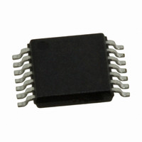
MAX5393NAUD+ Maxim Integrated Products, MAX5393NAUD+ Datasheet - Page 8

MAX5393NAUD+
Manufacturer Part Number
MAX5393NAUD+
Description
IC POT DGTL DUAL 256TAP 14TSSOP
Manufacturer
Maxim Integrated Products
Datasheet
1.MAX5391LATET.pdf
(14 pages)
Specifications of MAX5393NAUD+
Taps
256
Resistance (ohms)
100K
Number Of Circuits
2
Temperature Coefficient
35 ppm/°C Typical
Memory Type
Volatile
Interface
SPI, 3-Wire Serial
Voltage - Supply
1.7 V ~ 5.5 V
Operating Temperature
-40°C ~ 125°C
Mounting Type
Surface Mount
Package / Case
14-TSSOP
Resistance In Ohms
100K
Number Of Pots
Dual
Taps Per Pot
256
Resistance
200 Ohms
Wiper Memory
Volatile
Digital Interface
Serial (3-Wire, SPI)
Operating Supply Voltage
1.7 V to 5.5 V
Supply Current
27 uA
Maximum Operating Temperature
+ 125 C
Minimum Operating Temperature
- 40 C
Description/function
Dual Volatile Low Voltage Linear Taper Digital Potentiometer
Mounting Style
SMD/SMT
Supply Voltage (max)
5.5 V
Supply Voltage (min)
1.7 V
Tolerance
25 %
Lead Free Status / RoHS Status
Lead free / RoHS Compliant
Dual 256-Tap, Volatile, Low-Voltage
Linear Taper Digital Potentiometers
8
(TQFN-EP)
MAX5391
6, 11, 13
______________________________________________________________________________________
10
12
14
15
16
—
1
2
3
4
5
7
8
9
TOP VIEW
*EP = EXPOSED PAD
PIN
N.C.
MAX5393
WA
(TSSOP)
HA
LA
10
11
13
12
14
—
3
4
2
5
1
6
7
8
9
13
14
15
16
+
12
1
NAME
SCLK
GND
N.C.
BYP
V
DIN
WB
I.C.
WA
HB
CS
HA
LB
LA
EP
DD
MAX5391
11
2
Resistor B High Terminal. The voltage at HB can be higher or lower than the voltage at
LB. Current can flow into or out of HB.
Resistor B Wiper Terminal
Resistor B Low Terminal. The voltage at LB can be higher or lower than the voltage at HB.
Current can flow into or out of LB.
Internally Connected. Connect to GND.
Ground
No Connection. Not internally connected.
Internal Power-Supply Bypass. For additional charge-pump filtering, bypass to GND with
a capacitor close to the device.
Active-Low Chip-Select Input
Serial-Interface Data Input
Serial-Interface Clock Input
Power-Supply Input. Bypass V
Resistor A High Terminal. The voltage at HA can be higher or lower than the voltage at
LA. Current can flow into or out of HA.
Resistor A Wiper Terminal
Resistor A Low Terminal. The voltage at LA can be higher or lower than the voltage at HA.
Current can flow into or out of LA.
Exposed Pad (MAX5391 Only). Connect to GND.
10
3
*EP
9
4
8
7
6
5
CS
BYP
N.C.
GND
DD
to GND with a 0.1FF capacitor close to the device.
FUNCTION
TOP VIEW
GND
BYP
WB
I.C.
HB
CS
LB
1
4
5
6
7
2
3
+
MAX5393
Pin Configurations
Pin Description
14
13
12
11
10
9
8
LA
HA
WA
V
N.C.
SCLK
DIN
DD


