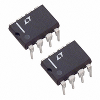
LTC1287CCN8 Linear Technology, LTC1287CCN8 Datasheet - Page 9

LTC1287CCN8
Manufacturer Part Number
LTC1287CCN8
Description
IC DATA ACQ SYS 12BIT 3V 8-DIP
Manufacturer
Linear Technology
Type
Data Acquisition System (DAS)r
Datasheet
1.LTC1287CCN8.pdf
(16 pages)
Specifications of LTC1287CCN8
Resolution (bits)
12 b
Sampling Rate (per Second)
30k
Data Interface
Serial, Parallel
Voltage Supply Source
Single Supply
Voltage - Supply
3V
Operating Temperature
0°C ~ 70°C
Mounting Type
Through Hole
Package / Case
8-DIP (0.300", 7.62mm)
Lead Free Status / RoHS Status
Contains lead / RoHS non-compliant
Available stocks
Company
Part Number
Manufacturer
Quantity
Price
Company:
Part Number:
LTC1287CCN8
Manufacturer:
TI
Quantity:
190
A
such as obtained from a voltage regulator (e.g., LT1117).
For high frequency bypassing a 0.1 F ceramic disk placed
in parallel with the 22 F is recommended. Again the leads
should be kept to a minimum. Using a battery to power the
LTC1287 will help reduce the amount of bypass capacitance
required on the V
device will only require 10 F to adequately bypass the
supply pin. Figure 4 shows the effect of poor V
Figure 5 shows the settling of a LT1117 low dropout
regulator with a 22 F bypass capacitor. The noise and
ripple is kept around 0.5mV. Figure 6 shows the response
of a lithium battery with a 10 F bypass capacitor. The
noise and ripple is kept below 0.5mV.
Analog Inputs
Because of the capacitive redistribution A/D conversion
techniques used, the analog inputs of the LTC1287 have
PPLICATI
0.5mV/DIV
Figure 5. LT1117 Regulator with 22 F Bypassing on V
5V/DIV
Figure 4. Poor V
Ripple Can Cause A/D Errors
O
CC
U
HORIZONTAL: 20 s/DIV
pin. A battery placed close to the
HORIZONTAL: 10 s/DIV
S
CC
I FOR ATIO
U
Bypassing. Noise and
W
CC
bypassing.
U
CS
V
CC
CC
capacitive switching input current spikes. These current
spikes settle quickly and do not cause a problem. If large
source resistances are used or if slow settling op amps
drive the inputs, take care to insure the transients caused
by the current spikes settle completely before the
conversion begins.
Source Resistance
The analog inputs of the LTC1287 look like a 100pF
capacitor (C
value for R
R
= – 2.7V, R
(+) and (–) inputs once during each conversion cycle.
Large external source resistors and capacitances will slow
the settling of the inputs. It is important that the overall RC
time constant is short enough to allow the analog inputs
to settle completely within the allowed time.
ON
0.5mV/DIV
V
Figure 6. Lithium Battery with 10 F Bypassing on V
will be reduced. For example, with V
V
IN
IN
5V/DIV
–
+
ON
ON
R
R
SOURCE
SOURCE
IN
Figure 7. Analog Input Equivalent Circuit
is for V
becomes 500 . C
) in series with a 1.5k resistor (R
+
–
CC
C1
INPUT
INPUT
C2
= 2.7V. With larger supply voltages
“+”
“–”
HORIZONTAL: 20 s/DIV
IN
gets switched between
CS
t
1/2 CLK
WHCS
R
ON
+
CC
= 1.5k
LTC1287
= 2.7V and V
LTC1287
C
100pF
IN
LTC1287 F07
ON
=
CC
CS
V
). This
CC
1287fa
9
–


