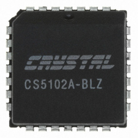
CS5102A-BLZ Cirrus Logic Inc, CS5102A-BLZ Datasheet - Page 24

CS5102A-BLZ
Manufacturer Part Number
CS5102A-BLZ
Description
IC ADC 16BIT 100/20KHZ 28-PLCC
Manufacturer
Cirrus Logic Inc
Datasheet
1.CS5101A-BL8Z.pdf
(39 pages)
Specifications of CS5102A-BLZ
Number Of Bits
16
Sampling Rate (per Second)
20k
Data Interface
Serial
Number Of Converters
1
Power Dissipation (max)
65mW
Voltage Supply Source
Analog and Digital, Dual ±
Operating Temperature
-40°C ~ 85°C
Mounting Type
Surface Mount
Package / Case
28-PLCC
Lead Free Status / RoHS Status
Lead free / RoHS Compliant
Other names
598-1079-5
Available stocks
Company
Part Number
Manufacturer
Quantity
Price
Company:
Part Number:
CS5102A-BLZ
Manufacturer:
Cirrus Logic Inc
Quantity:
10 000
Part Number:
CS5102A-BLZ
Manufacturer:
CRYSTAL
Quantity:
20 000
capacitor exhibits an impedance of less than 2 Ω at
frequencies greater than 16 kHz. A high-quality
tantalum capacitor in parallel with a smaller ceram-
ic capacitor is recommended.
Peaking in the reference's output impedance can
occur because of capacitive loading at its output.
Any peaking that might occur can be reduced by
placing a small resistor in series with the capaci-
tors. The equation in Figure 11 can be used to help
calculate the optimum value of R for a particular
reference. The term “f
peak in the output impedance of the reference be-
fore the resistor is added.
The CS5101A and CS5102A can operate with a
wide range of reference voltages, but signal-to-
noise performance is maximized by using as wide a
signal range as possible. The recommended refer-
ence voltage is 4.5 volts. The CS5101A and
CS5102A can actually accept reference voltages up
to the positive analog supply. However, the buffer's
offset may increase as the reference voltage ap-
proaches VA+ thereby increasing external drive re-
quirements at VREF. A 4.5V reference is the
maximum reference voltage recommended. This al-
lows 0.5V headroom for the internal reference buff-
er. Also, the buffer enlists the aid of an external
0.1 µF ceramic capacitor which must be tied be-
tween its output, REFBUF, and the negative analog
supply, VA-. For more information on references,
consult application note
AN004, Voltage References for CS5012A / CS5014 /CS5016 /
CS5101A / CS5102A / CS5126 Series of A/D
24
V
ref
10 µ F
Figure 11. Reference Connections
R
R*
+ V
ee
=
--------------------------------------------------------------- -
(
2π
0.01 µ F
-5V
⋅
(
C1
peak
0.1 µ F
+
20
21
23
” is the frequency of the
1
C2
V R E F
R E F B U F
V A-
) fpeak
⋅
C S 5101A
C S 5102A
Converters.
OR
)
6.2
The analog input terminal functions similarly to the
VREF input after each conversion when switching
into the track mode. During the first six master
clock cycles in the track mode, the buffered version
of the analog input is used for coarse-charging the
capacitor array. An additional period is required for
fine-charging directly from AIN to obtain the speci-
fied accuracy. Figure 12 shows this operation. Dur-
ing coarse-charge the charge on the capacitor
array first settles to the buffered version of the an-
alog input. This voltage may be offset from the ac-
tual input voltage. During fine-charge, the charge
then settles to the accurate unbuffered version.
Fine-charge settling is specified as a maximum of
1.125 µs (CS5101A) or 5.625 µs (CS5102A) for an
analog source impedance of less than 50 Ω. In ad-
dition, the comparator requires a source imped-
ance of less than 400 Ω around 2 MHz for stability.
The source impedance can be effectively reduced
at high frequencies by adding capacitance from
AIN to ground (typically 200 pF). However, high
DC source resistances will increase the input's RC
time constant and extend the necessary acquisi-
tion time. For more information on input amplifiers,
consult the application note,
AN006, Buffer Amplifiers for CS5012A / 14 / 16 / CS5101A /
CS5102A / CS5126 Series of A/D Converters.
6.3
The CS5101A and CS5102A include a SLEEP pin.
When SLEEP is active (low) each device will dissi-
pate very low power to retain its calibration memo-
2.0 M H z C lock
8 M H z C lo ck
+2 0 0
+1 0 0
-1 00
-2 00
-3 00
-4 00
0
Analog Input Connection
Sleep Mode Operation
Figure 12. Charge Settling Time
0 .2 5
1.0
C o a rse -C h a rg e
A cquisition Tim e (us)
CS5101A CS5102A
0 .5
2 .0
F ine -C h a rg e
0 .7 5
3 .0
DS45F6
1 .0
4 .0


