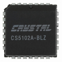
CS5102A-BLZ Cirrus Logic Inc, CS5102A-BLZ Datasheet - Page 23

CS5102A-BLZ
Manufacturer Part Number
CS5102A-BLZ
Description
IC ADC 16BIT 100/20KHZ 28-PLCC
Manufacturer
Cirrus Logic Inc
Datasheet
1.CS5101A-BL8Z.pdf
(39 pages)
Specifications of CS5102A-BLZ
Number Of Bits
16
Sampling Rate (per Second)
20k
Data Interface
Serial
Number Of Converters
1
Power Dissipation (max)
65mW
Voltage Supply Source
Analog and Digital, Dual ±
Operating Temperature
-40°C ~ 85°C
Mounting Type
Surface Mount
Package / Case
28-PLCC
Lead Free Status / RoHS Status
Lead free / RoHS Compliant
Other names
598-1079-5
Available stocks
Company
Part Number
Manufacturer
Quantity
Price
Company:
Part Number:
CS5102A-BLZ
Manufacturer:
Cirrus Logic Inc
Quantity:
10 000
Part Number:
CS5102A-BLZ
Manufacturer:
CRYSTAL
Quantity:
20 000
5.2
The CS5101A and CS5102A can alternatively be
used to sample one channel by tying the CH1/2 in-
put high or low. The unused AIN pin should be tied
to the analog input signal or to AGND. (If operating
in free run mode, AIN1 and AIN2 must be tied to
the same source, as CH1/2 is reconfigured as an
output.)
6. ANALOG CIRCUIT CONNECTIONS
Most popular successive approximation A/D con-
verters generate dynamic loads at their analog
connections. The CS5101A and CS5102A inter-
nally buffer all analog inputs (AIN1, AIN2, VREF,
and AGND) to ease the demands placed on exter-
nal circuitry. However, accurate system operation
still requires careful attention to details at the de-
sign stage regarding source impedances as well
as grounding and decoupling schemes.
6.1
An
References for the CS5012A / CS5014 /CS5016 /
verters
CS5102A. In addition to working through a refer-
ence circuit design example, it offers several built-
and-tested reference circuits.
During conversion, each capacitor of the calibrated
capacitor array is switched between VREF and
AGND in a manner determined by the successive-
approximation algorithm. The charging and dis-
charging of the array results in a current load at the
reference. The CS5101A and CS5102A each in-
DS45F6
CS5101A/ CS5102A / CS5126 Series of A/D Con
application
Single-channel Operation
Reference Considerations
Figure 10. Power-up Reset Circuit
is available for the CS5101A and
1N4148
+5V
note
R
C
titled
RST
VD+
CS5101A
CS5102A
AN004,
OR
Voltage
clude an internal buffer amplifier to minimize the
external reference circuit's drive requirement and
preserve the reference's integrity. Whenever the
array is switched during conversion, the buffer is
used to coarse-charge the array thereby providing
the bulk of the necessary charge. The appropriate
array capacitors are then switched to the unbuf-
fered VREF pin to avoid any errors due to offsets
and/or noise in the buffer.
The external reference circuitry need only provide
the residual charge required to fully charge the ar-
ray after coarse-charging from the buffer. This cre-
ates an ac current load as the CS5101A and
CS5102A sequence through conversions. The ref-
erence circuitry must have a low enough output im-
pedance to drive the requisite current without
changing its output voltage significantly. As the an-
alog input signal varies, the switching sequence of
the internal capacitor array changes. The current
load on the external reference circuitry thus varies
in response with the analog input. Therefore, the
external reference must not exhibit significant
peaking in its output impedance characteristic at
signal frequencies or their harmonics.
A large capacitor connected between VREF and
AGND can provide sufficiently low output imped-
ance at the high end of the frequency spectrum,
while almost all precision references exhibit ex-
tremely low output impedance at DC. The pres-
ence of large capacitors on the output of some
voltage references, however, may cause peaking
in the output impedance at intermediate frequen-
cies. Care should be exercised to ensure that sig-
nificant peaking does not exist or that some form of
compensation is provided to eliminate the effect.
The magnitude of the current load on the external
reference circuitry will scale to the master clock fre-
quency.
(CS5101A), the reference must supply a maximum
load current of 20 µA peak-to-peak (2 µA typical).
An output impedance of 2 Ω will therefore yield a
maximum error of 40 µV. At the full-rated 2.0 MHz
clock (CS5102A), the reference must supply a
maximum load current of 5 µA peak-to-peak
(0.5µA typical). An output impedance of 2 Ω will
therefore yield a maximum error of 10.0 µV. With a
4.5 V reference and LSB size of 138 µV this would
ensure approximately 1/14 LSB accuracy. A 10 µF
At
the
full-rated
CS5101A CS5102A
9.216 MHz
clock
23


