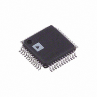
AD9244BSTZ-40 Analog Devices Inc, AD9244BSTZ-40 Datasheet - Page 6

AD9244BSTZ-40
Manufacturer Part Number
AD9244BSTZ-40
Description
IC ADC 14BIT 40MSPS 48-LQFP
Manufacturer
Analog Devices Inc
Datasheet
1.AD9244BSTZ-65.pdf
(36 pages)
Specifications of AD9244BSTZ-40
Data Interface
Parallel
Number Of Bits
14
Sampling Rate (per Second)
40M
Number Of Converters
1
Power Dissipation (max)
300mW
Voltage Supply Source
Analog and Digital
Operating Temperature
-40°C ~ 85°C
Mounting Type
Surface Mount
Package / Case
48-LQFP
Resolution (bits)
14bit
Sampling Rate
40MSPS
Input Channel Type
Differential, Single Ended
Supply Voltage Range - Analog
4.75V To 5.25V
Lead Free Status / RoHS Status
Lead free / RoHS Compliant
For Use With
AD9244-65PCBZ - BOARD EVAL FOR AD9244-65AD9244-40PCBZ - BOARD EVAL FOR AD9244-40
Lead Free Status / RoHS Status
Lead free / RoHS Compliant, Lead free / RoHS Compliant
Available stocks
Company
Part Number
Manufacturer
Quantity
Price
Company:
Part Number:
AD9244BSTZ-40
Manufacturer:
ADI
Quantity:
541
Company:
Part Number:
AD9244BSTZ-40
Manufacturer:
ADI
Quantity:
4
Company:
Part Number:
AD9244BSTZ-40
Manufacturer:
ADI
Quantity:
93
Company:
Part Number:
AD9244BSTZ-40
Manufacturer:
Analog Devices Inc
Quantity:
10 000
Part Number:
AD9244BSTZ-40
Manufacturer:
ADI/亚德诺
Quantity:
20 000
AD9244
Parameter
DIGITAL OUTPUTS (DRVDD = 3 V)
1
2
SWITCHING SPECIFICATIONS
AVDD = 5 V, DRVDD = 3 V, unless otherwise noted.
Table 4.
Parameter
CLOCK INPUT PARAMETERS
DATA OUTPUT PARAMETERS
OUT-OF-RANGE RECOVERY TIME
1
2
3
4
See the Clock Overview section for more details.
Output voltage levels measured with 5 pF load on each output.
The clock period can be extended to 2 μs with no degradation in specified performance at 25°C.
With duty cycle stabilizer enabled.
With duty cycle stabilizer disabled.
Measured from clock 50% transition to data 50% transition with 5 pF load on each output.
Logic 1 Voltage (I
Logic 0 Voltage (I
Logic 1 Voltage (I
Logic 0 Voltage (I
Maximum Conversion Rate
Minimum Conversion Rate
Clock Period
Clock Pulse Width High
Clock Pulse Width Low
Clock Pulse Width High
Clock Pulse Width Low
Output Delay (t
Pipeline Delay (Latency)
Aperture Delay (t
Aperture Uncertainty (Jitter)
Output Enable Delay
ANALOG INPUT
1
DATA OUT
PD
OH
OL
OH
OL
A
CLOCK
)
4
)
= 50 μA)
= 1.6 mA)
= 50 μA)
= 0.5 mA)
2
3
2
3
N – 9
N
2
N – 8
t
A
N + 1
N – 7
Temp
Full
Full
Full
Full
Full
Full
Full
Full
Full
Full
Full
Full
Full
N + 2
Temp
Full
Full
Full
Full
N – 6
N + 3
Test
Level
VI
V
V
V
V
V
V
V
V
V
V
V
V
Figure 2. Input Timing
N – 5
Rev. C | Page 6 of 36
Test
Level
IV
IV
IV
IV
N + 4
Min
65
15.4
4
4
6.9
6.9
3.5
N – 4
AD9244BST-65
Min
2.95
2.8
N + 5
2
Typ
8
1.5
0.3
15
AD9244BST-65
N – 3
Typ
N + 6
Max
500
7
N – 2
N + 7
Max
0.05
0.4
Min
40
25
4
4
11.3
11.3
3.5
N – 1
AD9244BST-40
N + 8
Min
2.95
2.8
Typ
8
1.5
0.3
15
1
AD9244BST-40
N
t
PD
N + 9
Typ
Max
500
7
N + 1
Max
0.05
0.4
Unit
MHz
kHz
ns
ns
ns
ns
ns
ns
Clock cycles
ns
ps rms
ns
Clock cycles
Unit
V
V
V
V


