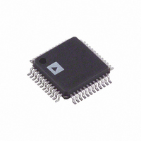
AD9244BSTZ-40 Analog Devices Inc, AD9244BSTZ-40 Datasheet - Page 22

AD9244BSTZ-40
Manufacturer Part Number
AD9244BSTZ-40
Description
IC ADC 14BIT 40MSPS 48-LQFP
Manufacturer
Analog Devices Inc
Datasheet
1.AD9244BSTZ-65.pdf
(36 pages)
Specifications of AD9244BSTZ-40
Data Interface
Parallel
Number Of Bits
14
Sampling Rate (per Second)
40M
Number Of Converters
1
Power Dissipation (max)
300mW
Voltage Supply Source
Analog and Digital
Operating Temperature
-40°C ~ 85°C
Mounting Type
Surface Mount
Package / Case
48-LQFP
Resolution (bits)
14bit
Sampling Rate
40MSPS
Input Channel Type
Differential, Single Ended
Supply Voltage Range - Analog
4.75V To 5.25V
Lead Free Status / RoHS Status
Lead free / RoHS Compliant
For Use With
AD9244-65PCBZ - BOARD EVAL FOR AD9244-65AD9244-40PCBZ - BOARD EVAL FOR AD9244-40
Lead Free Status / RoHS Status
Lead free / RoHS Compliant, Lead free / RoHS Compliant
Available stocks
Company
Part Number
Manufacturer
Quantity
Price
Company:
Part Number:
AD9244BSTZ-40
Manufacturer:
ADI
Quantity:
541
Company:
Part Number:
AD9244BSTZ-40
Manufacturer:
ADI
Quantity:
4
Company:
Part Number:
AD9244BSTZ-40
Manufacturer:
ADI
Quantity:
93
Company:
Part Number:
AD9244BSTZ-40
Manufacturer:
Analog Devices Inc
Quantity:
10 000
Part Number:
AD9244BSTZ-40
Manufacturer:
ADI/亚德诺
Quantity:
20 000
AD9244
Out of Range (OTR)
An out-of-range condition exists when the analog input voltage
is beyond the input range of the ADC. OTR is a digital output
that is updated along with the data output corresponding to the
particular sampled input voltage. Thus, OTR has the same pipe-
line latency as the digital data. OTR is low when the analog
input voltage is within the analog input range and high when
the analog input voltage exceeds the input range, as shown in
Figure 52. OTR remains high until the analog input returns to
within the input range and another conversion is completed.
By logically AND’ing OTR with the MSB and its complement,
overrange high or underrange low conditions can be detected.
Table 11 is a truth table for the overrange/underrange circuit in
Figure 53, which uses NAND gates. Systems requiring
programmable gain conditioning of the AD9244 can after eight
clock cycles detect an OTR condition, thus eliminating gain
selection iterations. In addition, OTR can be used for digital
offset and gain calibration.
Table 11. Output Data Format
OTR
0
0
1
1
MSB
MSB
OTR
OTR DATA OUTPUTS
1
0
0
0
0
1
Figure 52. OTR Relation to Input Voltage and Output Data
1111
1111
1111
0000
0000
0000
MSB
0
1
0
1
1111
1111
1111
0000
0000
0000
Figure 53. Overrange/Underrange Logic
1111
1111
1110
0001
0000
0000
–FS – 1/2 LSB
OTR
–FS
–FS + 1/2 LSB
Analog Input Is
Within range
Within range
Underrange
Overrange
+FS – 1/2 LSB
+FS – 1 LSB
OVER = 1
UNDER = 1
+FS
Rev. C | Page 22 of 36
Digital Output Enable Function (OEB)
The AD9244 has three-state ability. If the OEB pin is low, the
output data drivers are enabled. If the OEB pin is high, the out-
put data drivers are placed in a high impedance state. The
three-state ability is not intended for rapid access to the data
bus. Note that OEB is referenced to the digital supplies
(DRVDD) and should not exceed that supply voltage.
Clock Overview
The AD9244 has a flexible clock interface that accepts either a
single-ended or differential clock. An internal bias voltage
facilitates ac coupling using two external capacitors. To remain
backward compatible with the single-pin clock scheme of the
AD9226, the AD9244 can be operated with a dc-coupled,
single-pin clock by grounding the CLK− pin and driving CLK+.
When the CLK− pin is not grounded, the CLK+ and CLK– pins
function as a differential clock receiver. When CLK+ is greater
than CLK–, the SHA is in hold mode; when CLK+ is less than
CLK–, the SHA is in track mode (see Figure 54 for timing). The
rising edge of the clock (CLK+ – CLK–) switches the SHA from
track to hold, and timing jitter on this transition should be mini-
mized, especially for high frequency analog inputs.
It is often difficult to maintain a 50% duty cycle to the ADC,
especially when driving the clock with a single-ended or sine
wave input. To ease the constraint of providing an accurate 50%
clock, the ADC has an optional internal duty cycle stabilizer
(DCS) that allows the rising clock edge to pass through with
minimal jitter, and interpolates the falling edge, independent of
the input clock falling edge. The DCS is described in greater
detail in the Clock Stabilizer (DCS) section.
CLK–
CLK+
CLK–
CLK+
Figure 54. SHA Timing
SHA IN
HOLD
TRACK
SHA IN


