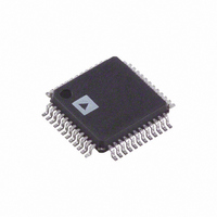
AD9244BSTZ-40 Analog Devices Inc, AD9244BSTZ-40 Datasheet - Page 17

AD9244BSTZ-40
Manufacturer Part Number
AD9244BSTZ-40
Description
IC ADC 14BIT 40MSPS 48-LQFP
Manufacturer
Analog Devices Inc
Datasheet
1.AD9244BSTZ-65.pdf
(36 pages)
Specifications of AD9244BSTZ-40
Data Interface
Parallel
Number Of Bits
14
Sampling Rate (per Second)
40M
Number Of Converters
1
Power Dissipation (max)
300mW
Voltage Supply Source
Analog and Digital
Operating Temperature
-40°C ~ 85°C
Mounting Type
Surface Mount
Package / Case
48-LQFP
Resolution (bits)
14bit
Sampling Rate
40MSPS
Input Channel Type
Differential, Single Ended
Supply Voltage Range - Analog
4.75V To 5.25V
Lead Free Status / RoHS Status
Lead free / RoHS Compliant
For Use With
AD9244-65PCBZ - BOARD EVAL FOR AD9244-65AD9244-40PCBZ - BOARD EVAL FOR AD9244-40
Lead Free Status / RoHS Status
Lead free / RoHS Compliant, Lead free / RoHS Compliant
Available stocks
Company
Part Number
Manufacturer
Quantity
Price
Company:
Part Number:
AD9244BSTZ-40
Manufacturer:
ADI
Quantity:
541
Company:
Part Number:
AD9244BSTZ-40
Manufacturer:
ADI
Quantity:
4
Company:
Part Number:
AD9244BSTZ-40
Manufacturer:
ADI
Quantity:
93
Company:
Part Number:
AD9244BSTZ-40
Manufacturer:
Analog Devices Inc
Quantity:
10 000
Part Number:
AD9244BSTZ-40
Manufacturer:
ADI/亚德诺
Quantity:
20 000
THEORY OF OPERATION
The AD9244 is a high performance, single-supply 14-bit ADC.
In addition to high dynamic range Nyquist sampling, it is
designed for excellent IF undersampling performance with an
analog input as high as 240 MHz.
The AD9244 uses a calibrated 10-stage pipeline architecture
with a patented, wideband, input sample-and-hold amplifier
(SHA) implemented on a cost-effective CMOS process. Each
stage of the pipeline, excluding the last, consists of a low resolu-
tion flash ADC along with a switched capacitor DAC and
interstage residue amplifier (MDAC). The MDAC amplifies the
difference between the reconstructed DAC output and the flash
input for the next stage in the pipeline. One bit of redundancy is
used in each of the stages to facilitate digital correction of flash
errors. The last stage simply consists of a flash ADC.
The pipeline architecture allows a greater throughput rate at the
expense of pipeline delay or latency. While the converter cap-
tures a new input sample every clock cycle, it takes eight clock
cycles for the conversion to be fully processed and appear at the
output, as illustrated in Figure 2. This latency is not a concern
in many applications. The digital output, together with the OTR
indicator, is latched into an output buffer to drive the output
pins. The output drivers of the AD9244 can be configured to
interface with 5 V or 3.3 V logic families.
The AD9244 has a duty clock stabilizer (DCS) that generates its
own internal falling edge to create an internal 50% duty cycle
clock, independent of the externally applied duty cycle. Control
of straight binary or twos complement output format is accom-
plished with the DFS pin.
The ADC samples the analog input on the rising edge of the
clock. While the clock is low, the input SHA is in sample mode.
When the clock transitions to a high logic level, the SHA goes
into the hold mode. System disturbances just prior to or imme-
diately after the rising edge of the clock and/or excessive clock
jitter can cause the SHA to acquire the wrong input value and
should be minimized.
ANALOG INPUT AND REFERENCE OVERVIEW
The differential input span of the AD9244 is equal to the poten-
tial at the VREF pin. The VREF potential can be obtained from
the internal AD9244 reference or an external source.
In differential applications, the center point of the input span is
the common-mode level of the input signals. In single-ended
applications, the center point is the dc potential applied to one
input pin while the signal is applied to the opposite input pin.
Figure 40 to Figure 42 show various system configurations.
Rev. C | Page 17 of 36
Figure 43 is a simplified model of the AD9244 analog input,
showing the relationship between the analog inputs, VIN+,
VIN–, and the reference voltage, VREF. Note that this is only a
symbolic model and that no actual negative voltages exist inside
the AD9244. Similar to the voltages applied to the top and bot-
tom of the resistor ladder in a flash ADC, the value VREF/2
defines the minimum and maximum input voltages to the
ADC core.
2.5V
1.5V
3.0V
2.0V
2.5V
1.5V
3.0V
2.0V
Figure 41. 2 V p-p Single-Ended Input, Common-Mode Voltage = 2 V
Figure 42. 2 V p-p Differential Input, Common-Mode Voltage = 2.5 V
Figure 40. 2 V p-p Differential Input, Common-Mode Voltage = 2 V
3.0V
2.0V
+
50V
50Ω
VIN+
VIN–
10μF
Figure 43. Equivalent Analog Input of AD9244
+
+
10μF
10μF
33Ω
33Ω
33Ω
20pF
0.1μF
33Ω
33Ω
+
–
2V
0.1pF
20pF
20pF
0.1μF
0.1μF
33Ω
V
VIN+
VIN–
VREF
SENSE
REFGND
AD9244
CORE
2.5V
2V
2V
AD9244
VIN+
VIN–
VREF
SENSE
REFGND
VIN+
VIN–
VREF
SENSE
REFGND
REFB
REFT
AD9244
AD9244
+VREF/2
–VREF/2
CORE
ADC
REFB
REFB
REFT
REFT
0.1μF
0.1μF
0.1μF
14
0.1μF
0.1μF
0.1μF
0.1μF
0.1μF
0.1μF
+
10μF
AD9244
+
+
10μF
10μF


