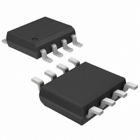
MAX1284BESA+ Maxim Integrated Products, MAX1284BESA+ Datasheet - Page 9

MAX1284BESA+
Manufacturer Part Number
MAX1284BESA+
Description
IC ADC 12BIT 400KSPS 8-SOIC
Manufacturer
Maxim Integrated Products
Datasheet
1.MAX1285BESA.pdf
(15 pages)
Specifications of MAX1284BESA+
Number Of Bits
12
Sampling Rate (per Second)
400k
Data Interface
MICROWIRE™, QSPI™, Serial, SPI™
Number Of Converters
1
Power Dissipation (max)
2.5mW
Voltage Supply Source
Single Supply
Operating Temperature
-40°C ~ 85°C
Mounting Type
Surface Mount
Package / Case
8-SOIC (0.154", 3.90mm Width)
Number Of Adc Inputs
1
Architecture
SAR
Conversion Rate
400 KSPs
Resolution
12 bit
Interface Type
Serial
Voltage Reference
Internal 2.5 V
Supply Voltage (max)
5 V
Mounting Style
SMD/SMT
Lead Free Status / RoHS Status
Lead free / RoHS Compliant
side of C
charges to the input signal again.
The time required for the T/H to acquire an input signal
is a function of how quickly its input capacitance is
charged. If the input signal’s source impedance is high,
the acquisition time lengthens and more time must be
allowed between conversions. The acquisition time
(t
the signal, and is also the minimum time needed for the
Figure 4. Equivalent Input Circuit
Figure 3. Typical Operating Circuit
ACQ
+5V OR +3V
AIN
ANALOG INPUT
*INCLUDES ALL INPUT PARASITICS
SHUTDOWN
) is the maximum time the device takes to acquire
0 TO V
400ksps/300ksps, Single-Supply, Low-Power,
INPUT
C
HOLD
REF
10μF
GND
SWITCH
REF
Serial 12-Bit ADCs with Internal Reference
6pF
*
0.1μF
switches back to AIN, and C
_______________________________________________________________________________________
CAPACITIVE DAC
HOLD
4.7μF
C
12pF
HOLD
1
2
3
4
V
AIN
SHDN
REF
DD
MAX1284
MAX1285
TRACK
R
800Ω
IN
ZERO
DOUT
SCLK
GND
CS
8
7
6
5
AUTOZERO
RAIL
COMPARATOR
SERIAL
INTERFACE
HOLD
signal to be acquired. Acquisition time is calculated by:
where R
impedance, and t
(MAX1284) or 625ns (MAX1285). Source impedances
below 2kΩ do not significantly affect the ADCs AC per-
formance.
Higher source impedances can be used if a 0.01µF
capacitor is connected to the analog input. Note that
the input capacitor forms an RC filter with the input
source impedance, limiting the ADCs input signal
bandwidth.
The ADCs’ input tracking circuitry has a 6MHz
(MAX1284) or 3MHz (MAX1285) small-signal band-
width, so it is possible to digitize high-speed transient
events and measure periodic signals with bandwidths
exceeding the ADC’s sampling rate, by using under-
sampling techniques. To avoid aliasing of unwanted
high-frequency signals into the frequency band of inter-
est, anti-alias filtering is recommended.
Internal protection diodes, which clamp the analog
input to V
(GND - 0.3V) to (V
If the analog input exceeds 50mV beyond the sup-
plies, limit the input current to 2mA.
The MAX1284/MAX1285 have an on-chip voltage refer-
ence trimmed to 2.5V. The internal reference output is
connected to REF and also drives the internal capaci-
tive DAC. The output can be used as a reference volt-
age source for other components and can source up to
800µA. Bypass REF with a 4.7µF capacitor. Larger
capacitors increase wake-up time when exiting shut-
down (see the Using SHDN to Reduce Supply Current
section). The internal reference is disabled in shutdown
(SHDN = 0).
When power is first applied, and if SHDN is not pulled
low, it takes the fully discharged 4.7µF reference
bypass capacitor up to 2ms to provide adequate
charge for specified accuracy. No conversions should
be performed during this time.
IN
DD
= 800Ω, R
t
Initialization after Power-Up and
and GND, allow the input to swing from
ACQ
DD
= 9(R
ACQ
+ 0.3V) without damage.
S
S
= the input signal’s source
+ R
is never less than 468ns
Starting a Conversion
IN
Analog Input Protection
Serial Interface
) x 12pF,
Internal Reference
Input Bandwidth
9


