MAX1284BESA+ Maxim Integrated Products, MAX1284BESA+ Datasheet - Page 10

MAX1284BESA+
Manufacturer Part Number
MAX1284BESA+
Description
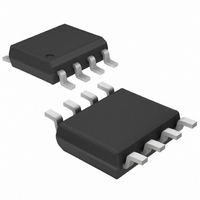
IC ADC 12BIT 400KSPS 8-SOIC
Manufacturer
Maxim Integrated Products
Datasheet
1.MAX1285BESA.pdf
(15 pages)
Specifications of MAX1284BESA+
Number Of Bits
12
Sampling Rate (per Second)
400k
Data Interface
MICROWIRE™, QSPI™, Serial, SPI™
Number Of Converters
1
Power Dissipation (max)
2.5mW
Voltage Supply Source
Single Supply
Operating Temperature
-40°C ~ 85°C
Mounting Type
Surface Mount
Package / Case
8-SOIC (0.154", 3.90mm Width)
Number Of Adc Inputs
1
Architecture
SAR
Conversion Rate
400 KSPs
Resolution
12 bit
Interface Type
Serial
Voltage Reference
Internal 2.5 V
Supply Voltage (max)
5 V
Mounting Style
SMD/SMT
Lead Free Status / RoHS Status
Lead free / RoHS Compliant
400ksps/300ksps, Single-Supply, Low-Power,
Serial 12-Bit ADCs with Internal Reference
Figure 5. Supply Current vs. Conversion Rate
Figure 6. Shutdown Sequence
10
To start a conversion, pull CS low. At CS’s falling edge,
the T/H enters its hold mode and a conversion is initiat-
ed. Data can then be shifted out serially with the exter-
nal clock.
Power consumption can be reduced significantly by
shutting down the MAX1284/MAX1285 between con-
versions. Figure 5 shows a plot of average supply cur-
rent versus conversion rate. The wake-up time (t
is the time from when SHDN is deasserted to the time
when a conversion may be initiated (Figure 6). This
time depends on the time in shutdown (Figure 7)
because the external 4.7µF reference bypass capacitor
loses charge slowly during shutdown and can be as
long as 2ms.
______________________________________________________________________________________
Using SHDN to Reduce Supply Current
100
10k
0.1
10
1k
1
SHDN
DOUT
0.1
CS
V
DOUT = FS
R
C
DD
L
L
= ∞
= 10pF
= 3V
1
CONVERSION RATE (ksps)
10
100
POWERED-UP
CONVERSION 0
1000 10,000 100,000
COMPLETE CONVERSION SEQUENCE
WAKE
POWERED-DOWN
)
Conversion-start and data-read operations are con-
trolled by the CS and SCLK digital inputs. The timing dia-
grams of Figures 8 and 9 outline serial-interface
operation.
A CS falling edge initiates a conversion sequence: the
T/H stage holds the input voltage, the ADC begins to
convert, and DOUT changes from high impedance to
logic low. SCLK is used to drive the conversion
process, and it shifts data out as each bit of conversion
is determined.
SCLK begins shifting out the data after the rising edge
of the third SCLK pulse. DOUT transitions 20ns after
each SCLK rising edge. The third rising clock edge
produces the MSB of the conversion at DOUT, followed
by the remaining bits. Since there are twelve data bits
and three leading zeros, at least fifteen rising clock
edges are needed to shift out these bits. Extra clock
pulses occurring after the conversion result has been
clocked out, and prior to a rising edge of CS, produce
trailing zeros at DOUT and have no effect on converter
operation.
Pull CS high after reading the conversion’s LSB. For
maximum throughout, CS can be pulled low again to
initiate the next conversion immediately after the speci-
fied minimum time (t
The data output from the MAX1284/MAX1285 is binary,
and Figure 10 depicts the nominal transfer function.
Code transitions occur halfway between successive-
integer LSB value V
2.5V/4096.
Output Coding and Transfer Function
t
WAKE
REF
CS
POWERED-UP
).
CONVERSION 1
= +2.5V, and 1LSB = 610µV or
Timing and Control


