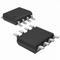
MAX1284BESA+ Maxim Integrated Products, MAX1284BESA+ Datasheet - Page 5

MAX1284BESA+
Manufacturer Part Number
MAX1284BESA+
Description
IC ADC 12BIT 400KSPS 8-SOIC
Manufacturer
Maxim Integrated Products
Datasheet
1.MAX1285BESA.pdf
(15 pages)
Specifications of MAX1284BESA+
Number Of Bits
12
Sampling Rate (per Second)
400k
Data Interface
MICROWIRE™, QSPI™, Serial, SPI™
Number Of Converters
1
Power Dissipation (max)
2.5mW
Voltage Supply Source
Single Supply
Operating Temperature
-40°C ~ 85°C
Mounting Type
Surface Mount
Package / Case
8-SOIC (0.154", 3.90mm Width)
Number Of Adc Inputs
1
Architecture
SAR
Conversion Rate
400 KSPs
Resolution
12 bit
Interface Type
Serial
Voltage Reference
Internal 2.5 V
Supply Voltage (max)
5 V
Mounting Style
SMD/SMT
Lead Free Status / RoHS Status
Lead free / RoHS Compliant
TIMING CHARACTERISTICS—MAX1284 (Figures 1, 2, 8, 9)
(V
TIMING CHARACTERISTICS—MAX1285 (Figures 1, 2, 8, 9)
(V
Note 1: Tested at V
Note 2: Relative accuracy is the deviation of the analog value at any code from its theoretical value after the full-scale range has
Note 3: Internal reference, offset, and reference errors nulled.
Note 4: Conversion time is defined as the number of clock cycles multiplied by the clock period; clock has 50% duty cycle.
Note 5: External load should not change during conversion for specified accuracy. Guaranteed specification limit of 2mV/mA due to
Note 6: Electrical characteristics are guaranteed from V
Note 7: MAX1284 tested with 20pF on D
SCLK Period
SCLK Pulse-Width High
SCLK Pulse-Width Low
CS Fall to SCLK Rise Setup
SCLK Rise to CS Rise Hold
SCLK Rise to CS Fall Ignore
CS Rise to SCLK Rise Ignore
SCLK Rise to DOUT Hold
SCLK Rise to DOUT Valid
CS Rise to DOUT Disable
CS Fall to DOUT Enable
CS Pulse-Width High
SCLK Period
SCLK Pulse-Width High
SCLK Pulse-Width Low
CS Fall to SCLK Rise Setup
SCLK Rise to CS Rise Hold
SCLK Rise to CS Fall Ignore
CS Rise to SCLK Rise Ignore
SCLK Rise to DOUT Hold
SCLK Rise to DOUT Valid
CS Rise to DOUT Disable
CS Fall to DOUT Enable
CS Pulse-Width High
DD
DD
= +4.5V to +5.5V, T
= +2.7V to +3.6V, T
been calibrated.
production test limitations.
Operating Characteristics .
0 to 3V. D
400ksps/300ksps, Single-Supply, Low-Power,
PARAMETER
PARAMETER
Serial 12-Bit ADCs with Internal Reference
OUT
DD
_______________________________________________________________________________________
= full scale.
= V
A
A
= T
= T
DD(MIN)
MIN
MIN
to T
to T
.
SYMBOL
SYMBOL
MAX,
MAX,
t
t
t
t
t
t
t
t
t
t
t
t
t
t
t
t
t
t
t
CSO
DOH
DOV
DOD
DOE
CSW
t
CSO
DOH
DOV
DOD
DOE
CSW
t
t
CSS
CSH
t
t
CSS
CSH
CS1
CS1
CH
CH
CP
CL
CP
CL
OUT
unless otherwise noted.)
unless otherwise noted.)
and f
C
C
C
C
C
C
C
C
LOAD
LOAD
LOAD
LOAD
LOAD
LOAD
LOAD
LOAD
SCLK
= 20pF
= 20pF
= 20pF
= 20pF
= 20pF
= 20pF
= 20pF
= 20pF
= 6.4MHz, 0 to 5V. MAX1285 tested with same loads, f
DD(MIN)
CONDITIONS
CONDITIONS
to V
DD(MAX)
. For operations beyond this range, see Typical
MIN
MIN
156
100
208
100
62
62
35
35
35
10
10
83
83
45
45
45
13
13
0
0
TYP
TYP
SCLK
MAX
MAX
100
= 4.8MHz,
80
65
65
85
85
UNITS
UNITS
ns
ns
ns
ns
ns
ns
ns
ns
ns
ns
ns
ns
ns
ns
ns
ns
ns
ns
ns
ns
ns
ns
ns
ns
5


