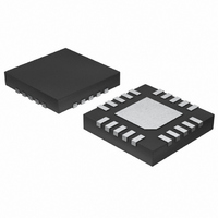
MAX1377ATP+ Maxim Integrated Products, MAX1377ATP+ Datasheet - Page 23

MAX1377ATP+
Manufacturer Part Number
MAX1377ATP+
Description
IC ADC 12BIT 1.25MSPS DL 20-TQFN
Manufacturer
Maxim Integrated Products
Datasheet
1.MAX1377ATP.pdf
(25 pages)
Specifications of MAX1377ATP+
Number Of Bits
12
Sampling Rate (per Second)
1.25M
Data Interface
DSP, MICROWIRE™, QSPI™, Serial, SPI™
Number Of Converters
2
Power Dissipation (max)
40mW
Voltage Supply Source
Single Supply
Operating Temperature
-40°C ~ 125°C
Mounting Type
Surface Mount
Package / Case
20-WQFN, Exposed Pad
Number Of Adc Inputs
2
Architecture
SAR
Conversion Rate
1.25 MSPs
Resolution
10 bit
Interface Type
Dual Serial
Voltage Reference
Internal 2.048 V or External
Supply Voltage (max)
3.3 V
Mounting Style
SMD/SMT
Lead Free Status / RoHS Status
Lead free / RoHS Compliant
Use the MAX1377/MAX1379/MAX1383 in a variety of
wireless communication systems. These devices allow
precise, simultaneous sampling of the I and Q signals
of quadrature RF receiver systems. Figure 17 shows the
MAX1377 in a simplified quadrature system. The device
has a differential input option that allows either full dif-
ferential or psuedo-differential signals. The 2:1 input
mux allows measurement of RSSI and other system-
monitoring functions with this device.
For best performance, use PCBs with ground planes.
Ensure that digital and analog signal lines are separat-
ed from each other. Do not run analog and digital
(especially clock) lines parallel to one another or digital
lines underneath the ADC package.
Establish a single-point analog ground (star ground point)
at AGND, separate from the digital ground, DGND.
Connect all other analog grounds and DGND to this star
ground point for further noise reduction. The ground return
to the power supply for this ground should be low imped-
ance and as short as possible for noise-free operation.
See Figure 14.
High-frequency noise in the AVDD power supply affects
the ADC’s high-speed comparator. Bypass the supply
to the single-point analog ground with 0.01µF and 10µF
bypass capacitors. Minimize capacitor lead lengths for
best supply-noise rejection.
Integral nonlinearity (INL) is the deviation of the values
on an actual transfer function from a straight line. This
straight line can be either a best-straight-line fit or a line
drawn between the end points of the transfer function,
once offset and gain errors have been nulled. The static
linearity parameters for the MAX1377/MAX1379/
MAX1383 are measured using the end-points method.
Differential nonlinearity (DNL) is the difference between
an actual step width and the ideal value of 1 LSB. A
DNL error specification of 1 LSB or less guarantees no
missing codes and a monotonic transfer function.
Aperture jitter (t
the time between the samples.
Dual, 12-Bit, 1.25Msps Simultaneous-Sampling
Layout, Grounding, and Bypassing
AJ
) is the sample-to-sample variation in
______________________________________________________________________________________
Wireless Communication
Differential Nonlinearity
Integral Nonlinearity
Aperture Jitter
Definitions
ADCs with Serial Interface
Aperture delay (t
falling edge of CNVST and the instant when an actual
sample is taken.
For a waveform perfectly reconstructed from digital
samples, signal-to-noise ratio (SNR) is the ratio of full-
scale analog input (RMS value) to the RMS quantization
error (residual error). The theoretical minimum analog-
to-digital noise is caused by quantization error, and
results directly from the ADC’s resolution (N bits):
In reality, there are other noise sources besides quanti-
zation noise, including thermal noise, reference noise,
clock jitter, etc. Therefore, SNR is computed by taking
the ratio of the RMS signal to the RMS noise, which
includes all spectral components minus the fundamen-
tal, the first five harmonics, and the DC offset.
Signal-to-noise plus distortion (SINAD) is the ratio of the
fundamental input frequency’s RMS amplitude to the
RMS equivalent of all other ADC output signals:
Effective number of bits (ENOB) indicates the global
accuracy of an ADC at a specific input frequency and
sampling rate. An ideal ADC’s error consists of quanti-
Figure 17. Quadrature Wireless-Communication System
T/R
SINAD(dB) = 20 x log(SignalRMS/NoiseRMS)
DEMODULATOR
TRANSMITTER
QUADRATURE
QUADRATURE
SNR = (6.02 x N + 1.76)dB
Signal-to-Noise Plus Distortion
AD
) is the time defined between the
I
Q
Effective Number of Bits
AVDD
Signal-to-Noise Ratio
MAX1377
V
12-BIT
12-BIT
DAC
DAC
ADC
ADC
L
Aperture Delay
PROCESSING
DSP
V
L
23


