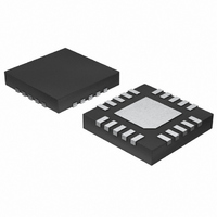
MAX1377ATP+ Maxim Integrated Products, MAX1377ATP+ Datasheet - Page 16

MAX1377ATP+
Manufacturer Part Number
MAX1377ATP+
Description
IC ADC 12BIT 1.25MSPS DL 20-TQFN
Manufacturer
Maxim Integrated Products
Datasheet
1.MAX1377ATP.pdf
(25 pages)
Specifications of MAX1377ATP+
Number Of Bits
12
Sampling Rate (per Second)
1.25M
Data Interface
DSP, MICROWIRE™, QSPI™, Serial, SPI™
Number Of Converters
2
Power Dissipation (max)
40mW
Voltage Supply Source
Single Supply
Operating Temperature
-40°C ~ 125°C
Mounting Type
Surface Mount
Package / Case
20-WQFN, Exposed Pad
Number Of Adc Inputs
2
Architecture
SAR
Conversion Rate
1.25 MSPs
Resolution
10 bit
Interface Type
Dual Serial
Voltage Reference
Internal 2.048 V or External
Supply Voltage (max)
3.3 V
Mounting Style
SMD/SMT
Lead Free Status / RoHS Status
Lead free / RoHS Compliant
Dual, 12-Bit, 1.25Msps Simultaneous-Sampling
ADCs with Serial Interface
the MAX1383, the signal bandwidth is limited to 100kHz
by specification. Since ±10V signals are divided down to
a 2.5V range, this version should only be used with sig-
nals greater than 5V. For those applications with signals
5V or less, use the MAX1377/MAX1379 for best SNR per-
formance. The configuration is shown on Figure 3b.
The ADC’s input-tracking circuitry has a 5MHz small-
signal bandwidth, allowing the ADC to digitize high-
speed transient events and measure periodic signals
with bandwidths exceeding the ADC’s sampling rate by
using undersampling techniques. To avoid high-fre-
quency signals being aliased into the frequency band
of interest, anti-alias filtering is recommended.
Internal protection diodes that clamp the analog input
to AVDD and AGND allow the analog inputs to swing
from AGND - 0.3V to AVDD + 0.3V without damage to
the MAX1377 and MAX1379. The MAX1383 can handle
Figure 3b. MAX1383 Equivalent Input Circuit
Figure 4a. MAX1377/MAX1379 Unipolar Transfer Function (U/B
= Low)
16
R
INTERNAL
IN
GROUND
SIGNAL
______________________________________________________________________________________
~ 11KΩ (typ)
INPUT
111...111
111...110
111...101
000...011
000...010
000...001
000...000
R1
0
REF (2.5V)
1
2
R2
3
INPUT VOLTAGE (LSB)
R4
Analog Input Protection
R3
FULL-SCALE
TRANSITION
Input Bandwidth
3pF
INA
FS - 3/2 LSB
1 LSB =
FS
ZS = 0
FS = V
V
4096
REF
REF
T/H
±10V input swings. All inputs must not exceed the stat-
ed ranges for accurate conversions.
Drive REFSEL low to select internal reference mode. The
MAX1377 includes an on-chip 2.048V reference; the
MAX1379 has a 4.096V reference; and the MAX1383
includes a 2.5V internal reference. The reference output
at REF can be used as a reference voltage source for
other components. REF can source up to 2mA. Bypass
REF with a 10nF capacitor and a 4.7µF capacitor to
RGND. It is important to select a low ESR capacitor and
keep the trace resistance as low as possible.
Figure 4b. MAX1383 Single-Ended Input
Figure 5. Bipolar Transfer Function (U/B = High)
100...001
100...000
011...111
011...100
000...010
000...001
000...000
111...111
111...110
111...101
111...111
111...110
111...101
000...011
000...010
000...001
000...000
-FS
-FS
DIFFERENTIAL INPUT VOLTAGE (LSB)
INPUT VOLTAGE (LSB)
Internal Reference Mode
V
V
REF
REF
- 1 LSB
- 1 LSB
FULL-SCALE
FULL-SCALE
TRANSITION
TRANSITION
1 LSB =
MAX1377/
MAX1379
MAX1383
+FS - 3/2 LSB
+FS = 4V
+FS - 3/2 LSB
1 LSB =
-FS = -4V
1 LSB =
ZS = 0
MAX1383
+FS
+FS
+FS =
+FS = 4V
-FS =
-FS = -4V
ZS = 0
ZS = 0
8 x V
4096
V
-V
REF
8 x V
V
4096
REF
REF
4096
2
REF
REF
2
REF
REF
REF
REF


