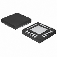
MAX1377ATP+ Maxim Integrated Products, MAX1377ATP+ Datasheet - Page 19

MAX1377ATP+
Manufacturer Part Number
MAX1377ATP+
Description
IC ADC 12BIT 1.25MSPS DL 20-TQFN
Manufacturer
Maxim Integrated Products
Datasheet
1.MAX1377ATP.pdf
(25 pages)
Specifications of MAX1377ATP+
Number Of Bits
12
Sampling Rate (per Second)
1.25M
Data Interface
DSP, MICROWIRE™, QSPI™, Serial, SPI™
Number Of Converters
2
Power Dissipation (max)
40mW
Voltage Supply Source
Single Supply
Operating Temperature
-40°C ~ 125°C
Mounting Type
Surface Mount
Package / Case
20-WQFN, Exposed Pad
Number Of Adc Inputs
2
Architecture
SAR
Conversion Rate
1.25 MSPs
Resolution
10 bit
Interface Type
Dual Serial
Voltage Reference
Internal 2.048 V or External
Supply Voltage (max)
3.3 V
Mounting Style
SMD/SMT
Lead Free Status / RoHS Status
Lead free / RoHS Compliant
In dual-output mode, conversion results from the two
channels appear on separate outputs. DOUT1 outputs
the result from channel 1 and DOUT2 outputs the result
from channel 2. Drive S/D low to operate in dual-output
mode. For DSPs with two-buffer and two-input-stream
capability, use the dual-output mode to allow for easier
DSP software for dual streams. Two buffer locations can
be used so the streams do not need to be separated.
In single-output mode, the results from both channels
appear on DOUT1. The channel 2 conversion result fol-
lows the channel 1 conversion result (see Figure 10).
The MSB (D11) of the channel 2 conversion result
appears on DOUT1 after the 16th rising edge of SCLK.
The LSB (D0) of the channel 2 conversion result
appears on DOUT1 after the 27th rising edge of SCLK
and is ready to be clocked in on the 28th rising edge of
SCLK. DOUT2 is high-impedance when S/D is high.
If CNVST goes high after the 28th rising edge of SCLK,
DOUT1 goes high impedance until the next conversion
is initiated (single-conversion mode). If CNVST goes
high after the 14th rising edge and before the 28th ris-
ing edge of SCLK, DOUT1 is actively driven low until
the next conversion results are ready (continuous- con-
version mode).
Note: In single-output mode, the conversion speed is
limited to 0.625Msps by the maximum SCLK.
Figure 10. Single-Output Mode, Single and Continuous Conversions
Dual, 12-Bit, 1.25Msps Simultaneous-Sampling
CONTINUOUS CONVERSION
(SINGLE OUTPUT)
DOUT1
SINGLE CONVERSION
(SINGLE OUTPUT)
CNVST
CNVST
DOUT1
SCLK
SCLK
0
1
1
0
0
0
0
0
______________________________________________________________________________________
D11 D10 D9 D8
Single-/Dual-Output Modes (S/D)
D11 D10 D9 D8
CONVERSION RESULT
CONVERSION RESULT
8
8
D7
D7
CHANNEL 1
CHANNEL 1
9
9
D6 D5 D4 D3 D2 D1 D0 D11 D10 D9 D8 D7 D6 D5 D4
D6 D5 D4 D3 D2 D1 D0 D11 D10 D9 D8 D7 D6 D5 D4
ADCs with Serial Interface
14
16
16
Reduce power consumption by placing the MAX1377/
MAX1379 in partial power-down mode. Partial power-
down mode is ideal for infrequent data sampling and
applications requiring fast wake-up times. Pull CNVST
high after the 3rd and before the 14th rising edge of
SCLK to place the device in partial power-down mode.
This reduces the analog supply current to 2mA. While
in partial power-down mode, the internal reference
remains enabled (if REFSEL = GND). Figure 11 shows
the timing sequence to enter partial power-down mode.
Full power-down mode is ideal for infrequent data sam-
pling and very low-supply current applications. To enter
full power-down mode, place the MAX1377/MAX1379/
MAX1383 first in partial power-down mode. Perform the
CNVST/SCLK sequence necessary to enter partial
power-down mode. Repeat the same sequence to enter
full power-down mode. In full power-down mode, the
internal reference is disabled to minimize power con-
sumption. Figure 12 shows the timing sequence to
enter full power-down mode.
Another way to enter the full power-down mode is to
drive CS high. If CS is high, the MAX1377/MAX1379/
MAX1383 act as if the full power-down sequence were
issued. To exit the CS-initiated power-down mode,
drive CS low. Allow 2ms for the reference to wake up
and settle before performing a conversion.
17
17
CONVERSION RESULT
CONVERSION RESULT
CHANNEL 2
CHANNEL 2
24
24
D3
D3
Full Power-Down Mode (FPD)
25
D2 D1 D0
Partial Power-Down (PPD)
D2 D1 D0
Power-Down Modes
27
28
28
HIGH-Z
19


