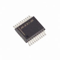
MAX1112CAP+ Maxim Integrated Products, MAX1112CAP+ Datasheet - Page 18

MAX1112CAP+
Manufacturer Part Number
MAX1112CAP+
Description
IC ADC 8-BIT 50KSPS 20-SSOP
Manufacturer
Maxim Integrated Products
Datasheet
1.MAX1113CEE.pdf
(20 pages)
Specifications of MAX1112CAP+
Number Of Bits
8
Sampling Rate (per Second)
50k
Data Interface
MICROWIRE™, QSPI™, Serial, SPI™
Number Of Converters
1
Power Dissipation (max)
680µW
Voltage Supply Source
Single Supply
Operating Temperature
0°C ~ 70°C
Mounting Type
Surface Mount
Package / Case
20-SSOP
Number Of Adc Inputs
8
Architecture
SAR
Conversion Rate
50 KSPs
Resolution
8 bit
Input Type
Differential
Interface Type
4-Wire (SPI, QSPI, MICROWIRE)
Voltage Reference
Internal 4.096 V or External
Supply Voltage (max)
5.5 V
Supply Voltage (min)
4.5 V
Maximum Power Dissipation
640 mW
Maximum Operating Temperature
+ 70 C
Mounting Style
SMD/SMT
Minimum Operating Temperature
0 C
Lead Free Status / RoHS Status
Lead free / RoHS Compliant
+5V, Low-Power, Multi-Channel,
Serial 8-Bit ADCs
Figure 15. Unipolar Transfer Function
Figure 16. Bipolar Transfer Function
18
11111111
11111110
00000011
00000010
11111101
00000001
00000000
01111111
01111110
00000010
00000001
00000000
11111111
11111110
11111101
10000001
10000000
______________________________________________________________________________________
OUTPUT CODE
(COM)
OUTPUT CODE
0
1
-FS
+FS =
1LSB =
COM =
-FS =
2
INPUT VOLTAGE (LSB)
V
-V
REFIN
V
V
3
2
REFIN
REFIN
256
REFIN
2
2
+ COM
+ COM
INPUT VOLTAGE (LSB)
FULL-SCALE
TRANSITION
COM
FS - 1LSB
1LSB =
FS = V
+FS -
FS
REFIN
1
2
V
REFIN
256
LSB
+ COM
For best performance, use printed circuit boards. Wire-
wrap boards are not recommended. Board layout
should ensure that digital and analog signal lines are
separated from each other. Do not run analog and digi-
tal (especially clock) lines parallel to one another, or
digital lines underneath the ADC package.
Figure 17 shows the recommended system ground
connections. A single-point analog ground (star ground
point) should be established at AGND, separate from
the logic ground. Connect all other analog grounds and
DGND to the star ground. No other digital system
ground should be connected to this ground. The
ground return to the power supply for the star ground
should be low impedance and as short as possible for
noise-free operation.
High-frequency noise in the V
affect the comparator in the ADC. Bypass the supply to
the star ground with 0.1µF and 1µF capacitors close to
the V
capacitor lead lengths for best supply-noise rejection. If
the +5V power supply is very noisy, a 10Ω resistor can
be connected to form a lowpass filter.
Figure 17. Power-Supply Grounding Connections
R* = 10
DD
* OPTIONAL
V
+5V
DD
pin of the MAX1112/MAX1113. Minimize
Layout, Grounding, and Bypassing
AGND
MAX1112
MAX1113
SUPPLIES
DD
DGND
power supply may
+5V
CIRCUITRY
DIGITAL
DGND
GND


