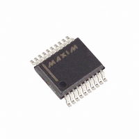
MAX1112CAP+ Maxim Integrated Products, MAX1112CAP+ Datasheet - Page 16

MAX1112CAP+
Manufacturer Part Number
MAX1112CAP+
Description
IC ADC 8-BIT 50KSPS 20-SSOP
Manufacturer
Maxim Integrated Products
Datasheet
1.MAX1113CEE.pdf
(20 pages)
Specifications of MAX1112CAP+
Number Of Bits
8
Sampling Rate (per Second)
50k
Data Interface
MICROWIRE™, QSPI™, Serial, SPI™
Number Of Converters
1
Power Dissipation (max)
680µW
Voltage Supply Source
Single Supply
Operating Temperature
0°C ~ 70°C
Mounting Type
Surface Mount
Package / Case
20-SSOP
Number Of Adc Inputs
8
Architecture
SAR
Conversion Rate
50 KSPs
Resolution
8 bit
Input Type
Differential
Interface Type
4-Wire (SPI, QSPI, MICROWIRE)
Voltage Reference
Internal 4.096 V or External
Supply Voltage (max)
5.5 V
Supply Voltage (min)
4.5 V
Maximum Power Dissipation
640 mW
Maximum Operating Temperature
+ 70 C
Mounting Style
SMD/SMT
Minimum Operating Temperature
0 C
Lead Free Status / RoHS Status
Lead free / RoHS Compliant
When power is first applied, and if SHDN is not pulled
low, internal power-on reset circuitry activates the
MAX1112/MAX1113 in internal clock mode. SSTRB is
high on power-up and, if CS is low, the first logical 1 on
DIN is interpreted as a start bit. Until a conversion takes
place, DOUT shifts out zeros. No conversions should
be performed until the reference voltage has stabilized
(see the Wakeup Time specifications in the Timing
Characteristics ).
When operating at speeds below the maximum sam-
pling rate, the MAX1112/MAX1113’s automatic power-
down mode can save considerable power by placing
the converters in a low-current shutdown state between
conversions. Figure 13 shows the average supply cur-
rent as a function of the sampling rate.
Select power-down with PD1 of the DIN control byte
with SHDN high or floating (Table 3). Pull SHDN low at
any time to shut down the converters completely. SHDN
overrides PD1 of the control byte. Figures 14a and 14b
illustrate the various power-down sequences in both
external and internal clock modes.
Software power-down is activated using bit PD1 of the
control byte. When software power-down is asserted, the
ADCs continue to operate in the last specified clock
mode until the conversion is complete. The ADCs then
power down into a low quiescent-current state. In internal
clock mode, the interface remains active, and conversion
results may be clocked out after the MAX1112/
MAX1113 have entered a software power-down.
The first logical 1 on DIN is interpreted as a start bit,
which powers up the MAX1112/MAX1113. If the DIN byte
contains PD1 = 1, then the chip remains powered up. If
PD1 = 0, power-down resumes after one conversion.
+5V, Low-Power, Multi-Channel,
Serial 8-Bit ADCs
Table 5. Hard-Wired Power-Down and
Internal Reference State
16
__________Applications Information
______________________________________________________________________________________
Floating
STATE
SHDN
1
0
Power-Down
DEVICE
Enabled
Enabled
MODE
Software Power-Down
Power-On Reset
Power-Down
REFERENCE
INTERNAL
Disabled
Disabled
Enabled
Pulling SHDN low places the converters in hard-wired
power-down. Unlike software power-down, the conver-
sion is not completed; it stops coincidentally with SHDN
being brought low. SHDN also controls the state of the
internal reference (Table 5). Letting SHDN float enables
the internal 4.096V voltage reference. When returning to
normal operation with SHDN floating, there is a t
delay of approximately 1MΩ x C
the capacitive loading on the SHDN pin. Pulling SHDN
high disables the internal reference, which saves power
when using an external reference.
An external reference between 1V and V
connected directly at the REFIN terminal. The DC input
impedance at REFIN is extremely high, consisting of
leakage current only (typically 10nA). During a conver-
sion, the reference must be able to deliver up to 20µA
average load current and have an output impedance of
1kΩ or less at the conversion clock frequency. If the
reference has higher output impedance or is noisy,
bypass it close to the REFIN pin with a 0.1µF capacitor.
If an external reference is used with the MAX1112/
MAX1113, tie SHDN to V
ence and decrease power consumption.
Figure 13. Average Supply Current vs. Sampling Rate
1000
100
10
0
C
CODE = 10101010
LOAD
10
= 60pF
C
CODE = 10101010
LOAD
SAMPLING RATE (ksps)
DD
= 30pF
20
V
C
DD
LOAD
to disable the internal refer-
Hard-Wired Power-Down
= V
External Reference
AT DOUT + SSTRB
REFIN
30
LOAD
C
CODE = 11111111
LOAD
= 5V
= 30pF
40
, where C
DD
50
should be
LOAD
RC
is


