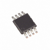
MAX11646EUA+ Maxim Integrated Products, MAX11646EUA+ Datasheet - Page 17

MAX11646EUA+
Manufacturer Part Number
MAX11646EUA+
Description
IC ADC 10BIT I2C 94.4KSPS 8UMAX
Manufacturer
Maxim Integrated Products
Datasheet
1.MAX11646EUA.pdf
(22 pages)
Specifications of MAX11646EUA+
Number Of Bits
10
Sampling Rate (per Second)
94.4k
Data Interface
I²C, Serial
Number Of Converters
1
Power Dissipation (max)
362mW
Voltage Supply Source
Single Supply
Operating Temperature
-40°C ~ 85°C
Mounting Type
Surface Mount
Package / Case
8-TSSOP, 8-MSOP (0.118", 3.00mm Width)
Number Of Adc Inputs
2
Conversion Rate
1 Ksps to 94.4 Ksps
Resolution
10 bit
Input Type
Single-Ended
Interface Type
I2C
Snr
60 dB
Voltage Reference
Internal 4.096 V
Supply Voltage (max)
5.5 V
Supply Voltage (min)
4.5 V
Maximum Power Dissipation
362 mW
Maximum Operating Temperature
+ 85 C
Input Voltage
4.5 V to 5.5 V
Minimum Operating Temperature
- 40 C
Lead Free Status / RoHS Status
Lead free / RoHS Compliant
When configured for external clock mode (CLK = 1),
the MAX11646/MAX11647 use the SCL as the conver-
sion clock. In external clock mode, the MAX11646/
MAX11647 begin tracking the analog input on the ninth
rising clock edge of a valid slave address byte. Two
SCL clock cycles later the analog signal is acquired
and the conversion begins. Unlike internal clock mode,
converted data is available immediately after the first
four empty high bits. The device continuously converts
input channels dictated by the scan mode until given a
not acknowledge. There is no need to re-address the
device with a read command to obtain new conversion
results (see Figure 11).
The conversion must complete in 1ms or droop on the
track-and-hold capacitor degrades conversion results.
Use internal clock mode if the SCL clock period
exceeds 60µs.
Figure 11. External Clock Mode Read Cycle
Table 5. Scanning Configuration
* When operating in external clock mode, there is no difference between SCAN[1:0] = 01 and SCAN[1:0] = 11, and converting occurs
perpetually until not acknowledge occurs.
SCAN1
B. SCAN MODE CONVERSIONS WITH EXTERNAL CLOCK
A. SINGLE CONVERSION WITH EXTERNAL CLOCK
1
S
1
S
0
0
1
1
SLAVE ADDRESS
SLAVE ADDRESS
MASTER TO SLAVE
SLAVE TO MASTER
7
7
SCAN0
0
1
0
1
Low-Power, 1-/2-Channel, I
1 1
R
1 1
R
______________________________________________________________________________________
A
A
Scans up from AIN0 to the input selected by CS0.
Converts the input selected by CS0 eight times (see Tables 3 and 4).*
Reserved. Do not use.
Converts input selected by CS0.*
t
t
ACQ
ACQ1
RESULT 1 (2 MSBs)
RESULT (2 MSBs)
in Ultra-Tiny 1.9mm x 2.2mm Package
8
8
1
A
1
A
t
CONV
t
CONV1
RESULT 2 (8 LSBs)
RESULT (8 LSBs)
External Clock
8
8
1
A
1
A
t
ACQ2
SCANNING CONFIGURATION
P OR Sr
1
The MAX11646/MAX11647 must operate in external
clock mode for conversion rates from 40ksps to
94.4ksps. Below 40ksps internal clock mode is recom-
mended due to much smaller power consumption.
SCAN0 and SCAN1 of the configuration byte set the
scan mode configuration. Table 5 shows the scanning
configurations. The scanned results are written to mem-
ory in the same order as the conversion. Read the
results from memory in the order they were converted.
Each result needs a 2-byte transmission, the first byte
begins with six empty bits during which SDA is left
high. Each byte has to be acknowledged by the master
or the memory transmission is terminated. It is not pos-
sible to read the memory independently of conversion.
RESULT N (2 MSBs)
t
ACQN
NUMBER OF BITS
8
1
A
t
2
CONVN
RESULT N (8 LSBs)
C, 10-Bit ADCs
8
1
A
P OR Sr
1
Scan Mode
NUMBER OF BITS
17


