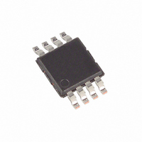
MAX11646EUA+ Maxim Integrated Products, MAX11646EUA+ Datasheet - Page 13

MAX11646EUA+
Manufacturer Part Number
MAX11646EUA+
Description
IC ADC 10BIT I2C 94.4KSPS 8UMAX
Manufacturer
Maxim Integrated Products
Datasheet
1.MAX11646EUA.pdf
(22 pages)
Specifications of MAX11646EUA+
Number Of Bits
10
Sampling Rate (per Second)
94.4k
Data Interface
I²C, Serial
Number Of Converters
1
Power Dissipation (max)
362mW
Voltage Supply Source
Single Supply
Operating Temperature
-40°C ~ 85°C
Mounting Type
Surface Mount
Package / Case
8-TSSOP, 8-MSOP (0.118", 3.00mm Width)
Number Of Adc Inputs
2
Conversion Rate
1 Ksps to 94.4 Ksps
Resolution
10 bit
Input Type
Single-Ended
Interface Type
I2C
Snr
60 dB
Voltage Reference
Internal 4.096 V
Supply Voltage (max)
5.5 V
Supply Voltage (min)
4.5 V
Maximum Power Dissipation
362 mW
Maximum Operating Temperature
+ 85 C
Input Voltage
4.5 V to 5.5 V
Minimum Operating Temperature
- 40 C
Lead Free Status / RoHS Status
Lead free / RoHS Compliant
A bus master initiates communication with a slave device
by issuing a START condition followed by a slave
address. When idle, the MAX11646/MAX11647 continu-
ously wait for a START condition followed by their slave
address. When the MAX11646/MAX11647 recognize their
slave address, they are ready to accept or send data.
The slave address has been factory programmed and is
always 0110110 for the MAX11646/MAX11647 (Figure 7).
The least significant bit (LSB) of the address byte (R/W)
determines whether the master is writing to or reading
from the MAX11646/MAX11647 (R/W = 0 selects a write
condition, R/W = 1 selects a read condition). After receiv-
ing the address, the MAX11646/MAX11647 (slave) issue
an acknowledge by pulling SDA low for one clock cycle.
At power-up, the MAX11646/MAX11647 bus timing is set
for fast mode (F/S mode), allowing conversion rates up to
22.2ksps. The MAX11646/MAX11647 must operate in
Figure 7. Slave Address Byte
Figure 8. F/S-Mode to HS-Mode Transfer
SDA
SCL
S
Low-Power, 1-/2-Channel, I
SDA
SCL
MAX11646/MAX11647
0
______________________________________________________________________________________
S
DEVICE
in Ultra-Tiny 1.9mm x 2.2mm Package
0
0
1
1
0
2
SLAVE ADDRESS
0110110
HS-MODE MASTER CODE
Slave Address
1
0
3
Bus Timing
SLAVE ADDRESS
F/S MODE
0
1
4
1
X
5
high-speed mode (HS mode) to achieve conversion
rates up to 94.4ksps. Figure 1 shows the bus timing for
the MAX11646/MAX11647’s 2-wire interface.
At power-up, the MAX11646/MAX11647 bus timing is
set for F/S mode. The bus master selects HS mode by
addressing all devices on the bus with the HS-mode
master code 0000 1XXX (X = don’t care). After suc-
cessfully receiving the HS-mode master code, the
MAX11646/MAX11647 issue a not-acknowledge, allow-
ing SDA to be pulled high for one clock cycle
(Figure 8). After the not-acknowledge, the MAX11646/
MAX11647 are in HS mode. The bus master must then
send a repeated START followed by a slave address to
initiate HS-mode communication. If the master gener-
ates a STOP condition the MAX11646/MAX11647 return
to F/S mode.
1
X
6
0
X
7
2
R/W
C, 10-Bit ADCs
A
8
A
9
Sr
HS MODE
HS Mode
13


