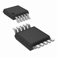
ADC124S021CIMM/NOPB National Semiconductor, ADC124S021CIMM/NOPB Datasheet - Page 17

ADC124S021CIMM/NOPB
Manufacturer Part Number
ADC124S021CIMM/NOPB
Description
IC ADC 12BIT 4CH 200KSPS 10MSOP
Manufacturer
National Semiconductor
Series
PowerWise®r
Datasheet
1.ADC124S021CIMMNOPB.pdf
(20 pages)
Specifications of ADC124S021CIMM/NOPB
Number Of Bits
12
Sampling Rate (per Second)
200k
Data Interface
DSP, MICROWIRE™, QSPI™, Serial, SPI™
Number Of Converters
1
Power Dissipation (max)
7.9mW
Voltage Supply Source
Single Supply
Operating Temperature
-40°C ~ 85°C
Mounting Type
Surface Mount
Package / Case
10-TFSOP, 10-MSOP (0.118", 3.00mm Width)
Number Of Elements
1
Resolution
12Bit
Architecture
SAR
Sample Rate
200KSPS
Input Polarity
Unipolar
Input Type
Voltage
Rated Input Volt
5.25V
Differential Input
No
Power Supply Requirement
Single
Single Supply Voltage (typ)
3.3/5V
Single Supply Voltage (min)
2.7V
Single Supply Voltage (max)
5.25V
Dual Supply Voltage (typ)
Not RequiredV
Dual Supply Voltage (min)
Not RequiredV
Dual Supply Voltage (max)
Not RequiredV
Power Dissipation
11mW
Differential Linearity Error
-0.8LSB/1.1LSB
Integral Nonlinearity Error
-1.1LSB/0.8LSB
Operating Temp Range
-40C to 85C
Operating Temperature Classification
Industrial
Mounting
Surface Mount
Pin Count
10
Package Type
MSOP
Input Signal Type
Single-Ended
For Use With
ADC124S021EVAL - BOARD EVALUATION FOR ADC124S021
Lead Free Status / RoHS Status
Lead free / RoHS Compliant
Other names
ADC124S021CIMM
ADC124S021CIMMTR
ADC124S021CIMMTR
Because the reference for the ADC124S021 is the supply
voltage, any noise on the supply will degrade device noise
performance. To keep noise off the supply, use a dedicated
linear regulator for this device, or provide sufficient decou-
pling from other circuitry to keep noise off the ADC124S021
5.0 ANALOG INPUTS
An equivalent circuit for one of the ADC124S021's input chan-
nels is shown in Figure 5. Diodes D1 and D2 provide ESD
protection for the analog inputs. At no time should any input
go beyond (V
diodes will begin conducting, which could result in erratic op-
eration. For this reason, these ESD diodes should NOT be
used to clamp the input signal.
The capacitor C1 in Figure 5 has a typical value of 3 pF, and
is mainly the package pin capacitance. Resistor R1 is the on
resistance of the multiplexer and track / hold switch, and is
typically 500 ohms. Capacitor C2 is the ADC124S021 sam-
pling capacitor, and is typically 30 pF. The ADC124S021 will
deliver best performance when driven by a low-impedance
source to eliminate distortion caused by the charging of the
sampling capacitance. This is especially important when us-
ing the ADC124S021 to sample AC signals. Also important
when sampling dynamic signals is a band-pass or low-pass
filter to reduce harmonics and noise, improving dynamic per-
formance.
6.0 DIGITAL INPUTS AND OUTPUTS
The ADC124S021's digital output DOUT is limited by, and
cannot exceed, the supply voltage, V
are not prone to latch-up and, and although not recommend-
ed, SCLK, CS and DIN may be asserted before V
any latch-up risk.
FIGURE 5. Equivalent Input Circuit
A
+ 300 mV) or (GND − 300 mV), as these ESD
A
. The digital input pins
FIGURE 4. Typical Application Circuit
20124314
A
without
17
supply pin. Because of the ADC124S021's low power re-
quirements, it is also possible to use a precision reference as
a power supply to maximize performance. The four-wire in-
terface is also shown connected to a microprocessor or DSP.
7.0 POWER SUPPLY CONSIDERATIONS
The ADC124S021 is fully powered-up whenever CS is low,
and fully powered-down whenever CS is high, with one ex-
ception: the ADC124S021 automatically enters power-down
mode between the 16th falling edge of a conversion and the
1st falling edge of the subsequent conversion (see Timing
Diagrams).
The ADC124S021 can perform multiple conversions back to
back; each conversion requires 16 SCLK cycles. The AD-
C124S021 will perform conversions continuously as long as
CS is held low.
The user may trade off throughput for power consumption by
simply performing fewer conversions per unit time. The Power
Consumption vs. Sample Rate curve in the Typical Perfor-
mance Curves section shows the typical power consumption
of the ADC124S021 versus throughput. To calculate the pow-
er consumption, simply multiply the fraction of time spent in
the normal mode by the normal mode power consumption ,
and add the fraction of time spent in shutdown mode multi-
plied by the shutdown mode power dissipation.
7.1 Power Management
When the ADC124S021 is operated continuously in normal
mode, the maximum throughput is f
be traded for power consumption by running f
imum 3.2 MHz and performing fewer conversions per unit
time, putting the ADC124S021 into shutdown mode between
conversions. A plot of typical power consumption versus
throughput is shown in the Typical Performance Curves sec-
tion. To calculate the power consumption for a given through-
put, multiply the fraction of time spent in the normal mode by
the normal mode power consumption and add the fraction of
time spent in shutdown mode multiplied by the shutdown
mode power consumption. Generally, the user will put the part
into normal mode and then put the part back into shutdown
mode. Note that the curve of power consumption vs. through-
put is nearly linear. This is because the power consumption
in the shutdown mode is so small that it can be ignored for all
practical purposes.
20124313
SCLK
/16. Throughput may
SCLK
www.national.com
at its max-


