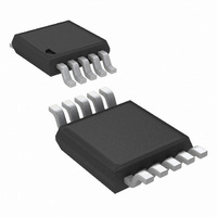
ADC124S021CIMM/NOPB National Semiconductor, ADC124S021CIMM/NOPB Datasheet - Page 15

ADC124S021CIMM/NOPB
Manufacturer Part Number
ADC124S021CIMM/NOPB
Description
IC ADC 12BIT 4CH 200KSPS 10MSOP
Manufacturer
National Semiconductor
Series
PowerWise®r
Datasheet
1.ADC124S021CIMMNOPB.pdf
(20 pages)
Specifications of ADC124S021CIMM/NOPB
Number Of Bits
12
Sampling Rate (per Second)
200k
Data Interface
DSP, MICROWIRE™, QSPI™, Serial, SPI™
Number Of Converters
1
Power Dissipation (max)
7.9mW
Voltage Supply Source
Single Supply
Operating Temperature
-40°C ~ 85°C
Mounting Type
Surface Mount
Package / Case
10-TFSOP, 10-MSOP (0.118", 3.00mm Width)
Number Of Elements
1
Resolution
12Bit
Architecture
SAR
Sample Rate
200KSPS
Input Polarity
Unipolar
Input Type
Voltage
Rated Input Volt
5.25V
Differential Input
No
Power Supply Requirement
Single
Single Supply Voltage (typ)
3.3/5V
Single Supply Voltage (min)
2.7V
Single Supply Voltage (max)
5.25V
Dual Supply Voltage (typ)
Not RequiredV
Dual Supply Voltage (min)
Not RequiredV
Dual Supply Voltage (max)
Not RequiredV
Power Dissipation
11mW
Differential Linearity Error
-0.8LSB/1.1LSB
Integral Nonlinearity Error
-1.1LSB/0.8LSB
Operating Temp Range
-40C to 85C
Operating Temperature Classification
Industrial
Mounting
Surface Mount
Pin Count
10
Package Type
MSOP
Input Signal Type
Single-Ended
For Use With
ADC124S021EVAL - BOARD EVALUATION FOR ADC124S021
Lead Free Status / RoHS Status
Lead free / RoHS Compliant
Other names
ADC124S021CIMM
ADC124S021CIMMTR
ADC124S021CIMMTR
Applications Information
1.0 ADC124S021 OPERATION
The ADC124S021 is a successive-approximation analog-to-
digital converter designed around a charge-redistribution dig-
ital-to-analog converter. Simplified schematics of the AD-
C124S021 in both track and hold modes are shown in
Figures 1, 2, respectively. In
track mode: switch SW1 connects the sampling capacitor to
one of four analog input channels through the multiplexer, and
SW2 balances the comparator inputs. The ADC124S021 is in
this state for the first three SCLK cycles after CS is brought
low.
Figure 2
connects the sampling capacitor to ground, maintaining the
2.0 USING THE ADC124S021
An ADC124S021 timing diagram and a serial interface timing
diagram for the ADC124S021 are shown in the Timing Dia-
grams section. CS is chip select, which initiates conversions
and frames the serial data transfers. SCLK (serial clock) con-
trols both the conversion process and the timing of serial data.
DOUT is the serial data output pin, where a conversion result
is sent as a serial data stream, MSB first. Data to be written
to the ADC124S021's Control Register is placed on DIN, the
serial data input pin. New data is written to the ADC at DIN
with each conversion.
A serial frame is initiated on the falling edge of CS and ends
on the rising edge of CS. Each frame must contain an integer
multiple of 16 rising SCLK edges. The ADC output data
(DOUT) is in a high impedance state when CS is high and is
active when CS is low. Thus, CS acts as an output enable.
shows the ADC124S021 in hold mode: switch SW1
Figure
1, the ADC124S021 is in
FIGURE 1. ADC124S021 in Track Mode
FIGURE 2. ADC124S021 in Hold Mode
15
sampled voltage, and switch SW2 unbalances the compara-
tor. The control logic then instructs the charge-redistribution
DAC to add fixed amounts of charge to the sampling capacitor
until the comparator is balanced. When the comparator is
balanced, the digital word supplied to the DAC is the digital
representation of the analog input voltage. The ADC124S021
is in this state for the fourth through sixteenth SCLK cycles
after CS is brought low.
The time when CS is low is considered a serial frame. Each
of these frames should contain an integer multiple of 16 SCLK
cycles, during which time a conversion is performed and
clocked out at the DOUT pin and data is clocked into the DIN
pin to indicate the multiplexer address for the next conversion.
Additionally, the device goes into a power down state when
CS is high, and also between continuous conversion cycles.
During the first 3 cycles of SCLK, the ADC is in the track
mode, acquiring the input voltage. For the next 13 SCLK cy-
cles the conversion is accomplished and the data is clocked
out, MSB first, starting on the 5th clock. If there is more than
one conversion in a frame, the ADC will re-enter the track
mode on the falling edge of SCLK after the N*16th rising edge
of SCLK, and re-enter the hold/convert mode on the N*16+4th
falling edge of SCLK, where "N" is an integer.
When CS is brought high, SCLK is internally gated off. If SCLK
is stopped in the low state while CS is high, the subsequent
fall of CS will generate a falling edge of the internal version of
SCLK, putting the ADC into the track mode. This is seen by
the ADC as the first falling edge of SCLK. If SCLK is stopped
with SCLK high, the ADC enters the track mode on the first
falling edge of SCLK after the falling edge of CS.
20124309
20124310
www.national.com


