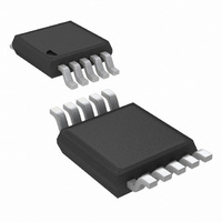
ADC124S021CIMM/NOPB National Semiconductor, ADC124S021CIMM/NOPB Datasheet - Page 16

ADC124S021CIMM/NOPB
Manufacturer Part Number
ADC124S021CIMM/NOPB
Description
IC ADC 12BIT 4CH 200KSPS 10MSOP
Manufacturer
National Semiconductor
Series
PowerWise®r
Datasheet
1.ADC124S021CIMMNOPB.pdf
(20 pages)
Specifications of ADC124S021CIMM/NOPB
Number Of Bits
12
Sampling Rate (per Second)
200k
Data Interface
DSP, MICROWIRE™, QSPI™, Serial, SPI™
Number Of Converters
1
Power Dissipation (max)
7.9mW
Voltage Supply Source
Single Supply
Operating Temperature
-40°C ~ 85°C
Mounting Type
Surface Mount
Package / Case
10-TFSOP, 10-MSOP (0.118", 3.00mm Width)
Number Of Elements
1
Resolution
12Bit
Architecture
SAR
Sample Rate
200KSPS
Input Polarity
Unipolar
Input Type
Voltage
Rated Input Volt
5.25V
Differential Input
No
Power Supply Requirement
Single
Single Supply Voltage (typ)
3.3/5V
Single Supply Voltage (min)
2.7V
Single Supply Voltage (max)
5.25V
Dual Supply Voltage (typ)
Not RequiredV
Dual Supply Voltage (min)
Not RequiredV
Dual Supply Voltage (max)
Not RequiredV
Power Dissipation
11mW
Differential Linearity Error
-0.8LSB/1.1LSB
Integral Nonlinearity Error
-1.1LSB/0.8LSB
Operating Temp Range
-40C to 85C
Operating Temperature Classification
Industrial
Mounting
Surface Mount
Pin Count
10
Package Type
MSOP
Input Signal Type
Single-Ended
For Use With
ADC124S021EVAL - BOARD EVALUATION FOR ADC124S021
Lead Free Status / RoHS Status
Lead free / RoHS Compliant
Other names
ADC124S021CIMM
ADC124S021CIMMTR
ADC124S021CIMMTR
www.national.com
During each conversion, data is clocked into the DIN pin on
the first 8 rising edges of SCLK after the fall of CS. For each
conversion, it is necessary to clock in the data indicating the
input that is selected for the conversion after the current one.
See Tables 1, 2 and 3.
If CS and SCLK go low within the times defined by t
t
DIN may be one clock cycle later than expected. It is, there-
3.0 ADC124S021 TRANSFER FUNCTION
The output format of the ADC124S021 is straight binary.
Code transitions occur midway between successive integer
LSB values. The LSB width for the ADC124S021 is V
4.0 TYPICAL APPLICATION CIRCUIT
A typical application of the ADC124S021 is shown in
4. Power is provided in this example by the National Semi-
conductor LP2950 low-dropout voltage regulator, available in
CLH
, the rising edge of SCLK that begins clocking data in at
Bit 7 (MSB)
DONTC
7 - 6, 2 - 0
Bit #:
5
4
3
DONTC
Symbol:
Bit 6
DONTC
ADD2
ADD1
ADD0
ADD2
TABLE 2. Control Register Bit Descriptions
Description
Don't care. The value of these bits do not affect device operation.
These three bits determine which input channel will be sampled and converted
in the next track/hold cycle. The mapping between codes and channels is shown
in
x
x
x
x
ADD2
FIGURE 3. Ideal Transfer Characteristic
Bit 5
Table
TABLE 3. Input Channel Selection
TABLE 1. Control Register Bits
3.
ADD1
CSU
A
0
0
1
1
Figure
/4096.
ADD1
and
Bit 4
16
ADD0
0
1
0
1
fore, best to strictly observe the minimum t
given in the Timing Specifications.
There are no power-up delays or dummy conversions re-
quired with the ADC124S021. The ADC is able to sample and
convert an input to full conversion immediately following pow-
er up. The first conversion result after power-up will be that of
IN1.
The ideal transfer characteristic is shown in Figure 3. The
transition from an output code of 0000 0000 0000 to a code
of 0000 0000 0001 is at 1/2 LSB, or a voltage of V
Other code transitions occur at steps of one LSB.
a variety of fixed and adjustable output voltages. The power
supply pin is bypassed with a capacitor network located close
to the ADC124S021.
ADD0
Bit 3
Input Channel
IN1 (Default)
IN2
IN3
IN4
DONTC
Bit 2
20124311
DONTC
Bit 1
CSU
and t
DONTC
Bit 0
CLH
A
/8192.
times


