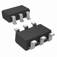
ADC121S021CIMF/NOPB National Semiconductor, ADC121S021CIMF/NOPB Datasheet - Page 5

ADC121S021CIMF/NOPB
Manufacturer Part Number
ADC121S021CIMF/NOPB
Description
ADC 12BIT 1CH 50-200KSPS SOT23-6
Manufacturer
National Semiconductor
Series
PowerWise®r
Datasheet
1.ADC121S021CIMFNOPB.pdf
(16 pages)
Specifications of ADC121S021CIMF/NOPB
Number Of Bits
12
Sampling Rate (per Second)
200k
Data Interface
DSP, MICROWIRE™, QSPI™, Serial, SPI™
Number Of Converters
1
Power Dissipation (max)
7.9mW
Voltage Supply Source
Single Supply
Operating Temperature
-40°C ~ 85°C
Mounting Type
Surface Mount
Package / Case
SOT-23-6
Lead Free Status / RoHS Status
Lead free / RoHS Compliant
Other names
ADC121S021CIMF
ADC121S021CIMFTR
ADC121S021CIMFTR
t
POWER-UP
Symbol
Symbol
ADC121S021 Timing Specifications
The following specifications apply for V
f
Note 1: Absolute Maximum Ratings indicate limits beyond which damage to the device may occur. Operating Ratings indicate conditions for which the device is
functional, but do not guarantee specific performance limits. For guaranteed specifications and test conditions, see the Electrical Characteristics. The guaranteed
specifications apply only for the test conditions listed. Some performance characteristics may degrade when the device is not operated under the listed test
conditions.
Note 2: All voltages are measured with respect to GND = 0V, unless otherwise specified.
Note 3: When the input voltage at any pin exceeds the power supply (that is, V
mA maximum package input current rating limits the number of pins that can safely exceed the power supplies with an input current of 10 mA to two. The Absolute
Maximum Rating specification does not apply to the V
Note 4: The absolute maximum junction temperature (T
junction-to-ambient thermal resistance (θ
for maximum power dissipation listed above will be reached only when the device is operated in a severe fault condition (e.g. when input or output pins are driven
beyond the power supply voltages, or the power supply polarity is reversed). Obviously, such conditions should always be avoided.
Note 5: Human body model is 100 pF capacitor discharged through a 1.5 kΩ resistor. Machine model is 220 pF discharged through zero ohms
Note 6: Reflow temperature profiles are different for lead-free and non-lead-free packages.
Note 7: Tested limits are guaranteed to National's AOQL (Average Outgoing Quality Level).
Note 8: This is the frequency range over which the electrical performance is guaranteed. The device is functional over a wider range which is specified under
Operating Ratings.
Note 9: Data sheet min/max specification limits are guaranteed by design, test, or statistical analysis.
Note 10: Minimum Quiet Time required by bus relinquish and the start of the next conversion.
Note 11: Measured with the timing test circuit shown in Figure 1 and defined as the time taken by the output signal to cross 1.0V.
Note 12: Measured with the timing test circuit shown in Figure 1 and defined as the time taken by the output signal to cross 1.0V or 2.0V.
Note 13: t
to remove the effects of charging or discharging the output capacitance. This means that t
SAMPLE
t
t
t
t
t
t
t
ACC
t
t
DIS
CH
t
AD
CS
SU
EN
CL
AJ
H
= 50 ksps to 200 ksps, Boldface limits apply for T
DIS
Minimum CS Pulse Width
CS to SCLK Setup Time
Delay from CS Until SDATA TRI-STATE
(Note
Data Access Time after SCLK Falling Edge
SCLK Low Pulse Width
SCLK High Pulse Width
SCLK to Data Valid Hold Time
SCLK Falling Edge to SDATA High Impedance
13)
Power-Up Time from Full Power-Down
Aperture Delay
Aperture Jitter
is derived from the time taken by the outputs to change by 0.5V with the timing test circuit shown in Figure 1. The measured number is then adjusted
11)
Parameter
Parameter
JA
), and the ambient temperature (T
A
= +2.7V to 5.25V, GND = 0V, f
A
pin. The current into the V
J
max) for this device is 150°C. The maximum allowable power dissipation is dictated by T
®
Disabled
(Note
(Note
12)
A
= T
A
), and can be calculated using the formula P
Conditions
5
IN
V
V
V
V
V
V
MIN
A
A
A
A
A
A
< GND or V
A
= +2.7V to +3.6V
= +4.75V to +5.25V
= +2.7V to +3.6V
= +4.75V to +5.25V
= +2.7V to +3.6V
= +4.75V to +5.25V
pin is limited by the Analog Supply Voltage specification.
to T
SCLK
Conditions
MAX
DIS
IN
is the true bus relinquish time, independent of the bus loading.
: all other limits T
= 1.0 MHz to 4.0 MHz, C
> V
A
), the current at that pin should be limited to 10 mA. The 20
Typical
A
30
Typical
3
= 25°C.
1
D
max = (T
L
= 25 pF,
(Note
Limits
0.4 x t
0.4 x t
J
max − T
Limits
10
10
20
40
20
25
25
9)
7
5
6
5
SCLK
SCLK
A
) / θ
www.national.com
JA
J
max, the
. The values
Units
ns (max)
ns (max)
ns (max)
ns (max)
ns (max)
ns (min)
ns (min)
ns (min)
ns (min)
ns (min)
ns (min)
ns (min)
ns (min)
ns
ps
Units
µs


