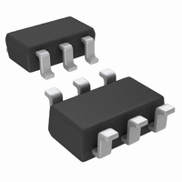
ADC121S021CIMF/NOPB National Semiconductor, ADC121S021CIMF/NOPB Datasheet - Page 12

ADC121S021CIMF/NOPB
Manufacturer Part Number
ADC121S021CIMF/NOPB
Description
ADC 12BIT 1CH 50-200KSPS SOT23-6
Manufacturer
National Semiconductor
Series
PowerWise®r
Datasheet
1.ADC121S021CIMFNOPB.pdf
(16 pages)
Specifications of ADC121S021CIMF/NOPB
Number Of Bits
12
Sampling Rate (per Second)
200k
Data Interface
DSP, MICROWIRE™, QSPI™, Serial, SPI™
Number Of Converters
1
Power Dissipation (max)
7.9mW
Voltage Supply Source
Single Supply
Operating Temperature
-40°C ~ 85°C
Mounting Type
Surface Mount
Package / Case
SOT-23-6
Lead Free Status / RoHS Status
Lead free / RoHS Compliant
Other names
ADC121S021CIMF
ADC121S021CIMFTR
ADC121S021CIMFTR
www.national.com
5.0 ANALOG INPUTS
An equivalent circuit for the ADC's input is shown in
7. Diodes D1 and D2 provide ESD protection for the analog
inputs. At no time should the analog input go beyond (V
300 mV) or (GND − 300 mV), as these ESD diodes will begin
to conduct, which could result in erratic operation. For this
reason, the ESD diodes should not be used to clamp the input
signal.
The capacitor C1 in
is mainly the package pin capacitance. Resistor R1 is the on
resistance of the track / hold switch, and is typically 500Ω.
Capacitor C2 is the ADC sampling capacitor and is typically
26 pF. The ADC will deliver best performance when driven by
a low-impedance source to eliminate distortion caused by the
charging of the sampling capacitance. This is especially im-
portant when using the ADC to sample AC signals. Also
important when sampling dynamic signals is an anti-aliasing
filter.
6.0 DIGITAL INPUTS AND OUTPUTS
The ADC digital inputs (SCLK and CS) are not limited by the
same maximum ratings as the analog inputs. The digital input
pins are instead limited to +5.25V with respect to GND, re-
gardless of V
interfaced with a wide range of logic levels, independent of
the supply voltage.
7.0 MODES OF OPERATION
The ADC has two possible modes of operation: normal mode,
and shutdown mode. The ADC enters normal mode (and a
FIGURE 7. Equivalent Input Circuit
A
, the supply voltage. This allows the ADC to be
Figure 7
has a typical value of 4 pF, and
FIGURE 6. Typical Application Circuit
20145114
Figure
A
+
12
conversion process is begun) when CS is pulled low. The de-
vice will enter shutdown mode if CS is pulled high before the
tenth falling edge of SCLK after CS is pulled low, or will stay
in normal mode if CS remains low. Once in shutdown mode,
the device will stay there until CS is brought low again. By
varying the ratio of time spent in the normal and shutdown
modes, a system may trade-off throughput for power con-
sumption, with a sample rate as low as zero.
7.1 Normal Mode
The fastest possible throughput is obtained by leaving the
ADC in normal mode at all times, so there are no power-up
delays. To keep the device in normal mode continuously,
CS must be kept low until after the 10th falling edge of SCLK
after the start of a conversion (remember that a conversion is
initiated by bringing CS low).
If CS is brought high after the 10th falling edge, but before the
16th falling edge, the device will remain in normal mode, but
the current conversion will be aborted, and SDATA will return
to TRI-STATE (truncating the output word).
Sixteen SCLK cycles are required to read all of a conversion
word from the device. After sixteen SCLK cycles have
elapsed, CS may be idled either high or low until the next
conversion. If CS is idled low, it must be brought high again
before the start of the next conversion, which begins when
CS is again brought low.
After sixteen SCLK cycles, SDATA returns to TRI-STATE.
Another conversion may be started, after t
by bringing CS low again.
7.2 Shutdown Mode
Shutdown mode is appropriate for applications that either do
not sample continuously, or it is acceptable to trade through-
put for power consumption. When the ADC is in shutdown
mode, all of the analog circuitry is turned off.
To enter shutdown mode, a conversion must be interrupted
by bringing CS high anytime between the second and tenth
falling edges of SCLK, as shown in
been brought high in this manner, the device will enter shut-
down mode; the current conversion will be aborted and SDA-
TA will enter TRI-STATE. If CS is brought high before the
second falling edge of SCLK, the device will not change
mode; this is to avoid accidentally changing mode as a result
of noise on the CS line.
20145113
Figure
QUIET
8. Once CS has
has elapsed,


