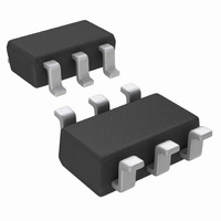
ADC121S021CIMF/NOPB National Semiconductor, ADC121S021CIMF/NOPB Datasheet - Page 2

ADC121S021CIMF/NOPB
Manufacturer Part Number
ADC121S021CIMF/NOPB
Description
ADC 12BIT 1CH 50-200KSPS SOT23-6
Manufacturer
National Semiconductor
Series
PowerWise®r
Datasheet
1.ADC121S021CIMFNOPB.pdf
(16 pages)
Specifications of ADC121S021CIMF/NOPB
Number Of Bits
12
Sampling Rate (per Second)
200k
Data Interface
DSP, MICROWIRE™, QSPI™, Serial, SPI™
Number Of Converters
1
Power Dissipation (max)
7.9mW
Voltage Supply Source
Single Supply
Operating Temperature
-40°C ~ 85°C
Mounting Type
Surface Mount
Package / Case
SOT-23-6
Lead Free Status / RoHS Status
Lead free / RoHS Compliant
Other names
ADC121S021CIMF
ADC121S021CIMFTR
ADC121S021CIMFTR
www.national.com
ANALOG I/O
DIGITAL I/O
POWER SUPPLY
Pin No.
Block Diagram
Pin Descriptions and Equivalent Circuits
PAD
3
4
5
6
1
2
Symbol
SDATA
SCLK
GND
GND
V
CS
V
IN
A
Analog input. This signal can range from 0V to V
Digital clock input. This clock directly controls the conversion and readout processes.
Digital data output. The output samples are clocked out of this pin on falling edges of the SCLK pin.
Chip select. On the falling edge of CS, a conversion process begins.
Positive supply pin. This pin should be connected to a quiet +2.7V to +5.25V source and bypassed to
GND with a 1 µF capacitor and a 0.1 µF monolithic capacitor located within 1 cm of the power pin.
The ground return for the supply and signals.
For package suffix CISD(X) only, it is recommended that the center pad should be connected to ground.
2
Description
A
.
20145107


