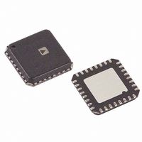
AD9245BCPZ-80 Analog Devices Inc, AD9245BCPZ-80 Datasheet - Page 21

AD9245BCPZ-80
Manufacturer Part Number
AD9245BCPZ-80
Description
IC ADC 14BIT 80MSPS 3V 32-LFCSP
Manufacturer
Analog Devices Inc
Datasheet
1.AD9245BCPZ-80.pdf
(32 pages)
Specifications of AD9245BCPZ-80
Data Interface
Parallel
Number Of Bits
14
Sampling Rate (per Second)
80M
Number Of Converters
3
Power Dissipation (max)
414mW
Voltage Supply Source
Single Supply
Operating Temperature
-40°C ~ 85°C
Mounting Type
Surface Mount
Package / Case
32-VFQFN, CSP Exposed Pad
Resolution (bits)
14bit
Sampling Rate
80MSPS
Input Channel Type
Differential, Single Ended
Supply Voltage Range - Analog
2.7V To 3.6V
Supply Current
122mA
Lead Free Status / RoHS Status
Lead free / RoHS Compliant
For Use With
AD9245BCP-80EBZ - BOARD EVAL FOR AD9245BCP-80AD9245BCP-40EBZ - BOARD EVAL FOR AD9245BCP-40AD9245BCP-20EBZ - BOARD EVAL FOR AD9245BCP-20
Lead Free Status / RoHS Status
Lead free / RoHS Compliant, Lead free / RoHS Compliant
Available stocks
Company
Part Number
Manufacturer
Quantity
Price
Company:
Part Number:
AD9245BCPZ-80
Manufacturer:
AD
Quantity:
197
Company:
Part Number:
AD9245BCPZ-80
Manufacturer:
ADI
Quantity:
1
Part Number:
AD9245BCPZ-80
Manufacturer:
ADI/亚德诺
Quantity:
20 000
As detailed in Table 11, the data format can be selected for either
offset binary or twos complement.
TIMING
The AD9245 provides latched data outputs with a pipeline delay
of seven clock cycles. Data outputs are available one propagation
delay (t
Figure 2 for a detailed timing diagram.
The length of the output data lines and the loads placed on
them should be minimized to reduce transients within the
AD9245. These transients can degrade the converter’s dynamic
performance.
The lowest typical conversion rate of the AD9245 is 1 MSPS. At
clock rates below 1 MSPS, dynamic performance can degrade.
VOLTAGE REFERENCE
A stable and accurate 0.5 V voltage reference is built into the
AD9245. The input range can be adjusted by varying the
reference voltage applied to the AD9245 using either the
internal reference or an externally applied reference voltage.
The input span of the ADC tracks reference voltage changes
linearly. The various reference modes are summarized in Table 10
and described in the following sections.
If the ADC is being driven differentially through a transformer,
the reference voltage can be used to bias the center tap
(common-mode voltage).
INTERNAL REFERENCE CONNECTION
A comparator within the AD9245 detects the potential at the
SENSE pin and configures the reference into one of four
possible states, which are summarized in Table 10. If SENSE is
grounded, the reference amplifier switch is connected to the
internal resistor divider (see Figure 45), setting VREF to 1 V.
Connecting the SENSE pin to VREF switches the reference
amplifier output to the SENSE pin, completing the loop and
providing a 0.5 V reference output. If a resistor divider is
connected as shown in Figure 47, the switch is again set to the
SENSE pin. This puts the reference amplifier in a noninverting
mode with the VREF output defined as
Table 10. Reference Configuration Summary
Selected Mode
External Reference
Internal Fixed Reference
Programmable Reference
Internal Fixed Reference
VREF
PD
) after the rising edge of the clock signal. Refer to
=
0
5 .
×
⎛ +
⎜
⎝
1
R2
R1
⎞
⎟
⎠
SENSE Voltage
AVDD
VREF
0.2 V to VREF
AGND to 0.2 V
Resulting VREF (V)
N/A
0.5
1.0
0.5
×
Rev. D | Page 21 of 32
⎛ +
⎜
⎝
1
R2
R1
⎞
⎟
⎠
(See Figure 47)
In all reference configurations, REFT and REFB drive the A/D
conversion core and establish its input span. The input range of
the ADC always equals twice the voltage at the reference pin for
either an internal or an external reference.
10μF
If the internal reference of the AD9245 is used to drive multiple
converters to improve gain matching, the loading of the reference
by the other converters must be considered. Figure 46 depicts
how the internal reference voltage is affected by loading. A
2 mA load is the maximum recommended load.
+
–0.05
–0.10
–0.15
–0.20
–0.25
0.05
0.1μF
0
0
SENSE
VREF
VIN+
VIN–
Figure 45. Internal Reference Configuration
0.5
Figure 46. VREF Accuracy vs. Load
Resulting Differential Span (V p-p)
2 × External Reference
1.0
2 × VREF
2.0
SELECT
LOGIC
1.0V ERROR (%)
1.0
AD9245
LOAD (mA)
1.5
0.5V
CORE
ADC
0.5V ERROR (%)
2.0
REFT
REFB
0.1μF
0.1μF
0.1μF
2.5
AD9245
+
10μF
3.0


