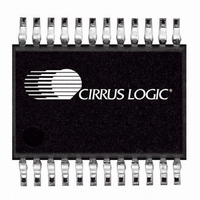
CS5566-ISZ Cirrus Logic Inc, CS5566-ISZ Datasheet - Page 17

CS5566-ISZ
Manufacturer Part Number
CS5566-ISZ
Description
IC ADC 24BIT 1CH 5KSPS 24SSOP
Manufacturer
Cirrus Logic Inc
Datasheet
1.CS5566-ISZ.pdf
(30 pages)
Specifications of CS5566-ISZ
Package / Case
24-SSOP
Number Of Bits
24
Data Interface
Serial
Number Of Converters
1
Voltage Supply Source
Dual ±
Operating Temperature
-40°C ~ 85°C
Mounting Type
Surface Mount
Architecture
Delta-Sigma
Conversion Rate
50 KSPs
Input Type
Voltage
Maximum Operating Temperature
+ 85 C
Mounting Style
SMD/SMT
Minimum Operating Temperature
- 40 C
Lead Free Status / RoHS Status
Lead free / RoHS Compliant
For Use With
598-1557 - BOARD EVAL FOR CS5566 ADC
Lead Free Status / Rohs Status
Lead free / RoHS Compliant
Other names
598-1269-5
Available stocks
Company
Part Number
Manufacturer
Quantity
Price
Company:
Part Number:
CS5566-ISZ
Manufacturer:
CIRRUS
Quantity:
76
3.5 Analog Input
The analog input of the converter is fully differential with a peak-to-peak input of 4.096 volts on each input.
Therefore, the differential, peak-to-peak input is 8.192 volts. This is illustrated in
These diagrams also illustrate a differential buffer amplifier configuration for driving the CS5566.
The capacitors at the outputs of the amplifiers provide a charge reservoir for the dynamic current from the
A/D inputs while the resistors isolate the dynamic current from the amplifier. The amplifiers can be pow-
ered from higher supplies than those used by the A/D but precautions should be taken to ensure that the
opamp output voltage remains within the power supply limits of the A/D, especially under start-up condi-
tions.
3.6 Output Coding Format
The reference voltage directly defines the input voltage range in both the unipolar and bipolar configura-
tions. In the unipolar configuration (BP/UP low), the first code transition occurs 0.5 LSB above zero, and
the final code transition occurs 1.5 LSBs below VREF. In the bipolar configuration (BP/UP high), the first
code transition occurs 0.5 LSB above -VREF and the last transition occurs 1.5 LSBs below +VREF. See
Table 1
DS806PP1
NOTE: VREF = (VREF+) - (VREF-)
NOTE: VREF = (VREF+) - (VREF-)
for the output coding of the converter.
Table 1. Output Coding, Two’s Complement
Unipolar Input Voltage
Bipolar Input Voltage
Table 2. Output Coding, Offset Binary
<(-VREF+0.5 LSB)
(VREF/2)-0.5 LSB
>(VREF-1.5 LSB)
>(VREF-1.5 LSB)
-VREF+0.5 LSB
VREF-1.5 LSB
VREF-1.5 LSB
<(+0.5 LSB)
+0.5 LSB
-0.5 LSB
3/25/08
Complement
7F FF FF
7F FF FE
FF FF FF
FF FF FF
FF FF FF
FF FF FE
7F FF FF
7F FF FF
00 00 00
80 00 01
80 00 00
80 00 00
80 00 00
00 00 01
00 00 00
00 00 00
Binary
Offset
Two’s
Figure 8
and
CS5566
Figure
17
9.


