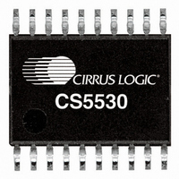
CS5530-ISZ Cirrus Logic Inc, CS5530-ISZ Datasheet - Page 23

CS5530-ISZ
Manufacturer Part Number
CS5530-ISZ
Description
IC ADC 24BIT 1CH W/LNA 20SSOP
Manufacturer
Cirrus Logic Inc
Datasheet
1.CS5530-ISZ.pdf
(36 pages)
Specifications of CS5530-ISZ
Number Of Converters
1
Package / Case
20-SSOP
Number Of Bits
24
Sampling Rate (per Second)
3.84k
Data Interface
Serial
Power Dissipation (max)
45mW
Voltage Supply Source
Analog and Digital, Dual ±
Operating Temperature
-40°C ~ 85°C
Mounting Type
Surface Mount
Number Of Adc Inputs
1
Architecture
Delta-Sigma
Conversion Rate
6.25 SPs to 3840 SPs
Resolution
24 bit
Input Type
Voltage
Interface Type
Serial (3-Wire)
Voltage Reference
2.5 V
Maximum Power Dissipation
500 mW
Maximum Operating Temperature
+ 85 C
Mounting Style
SMD/SMT
Minimum Operating Temperature
- 40 C
Lead Free Status / RoHS Status
Lead free / RoHS Compliant
For Use With
598-1158 - BOARD EVAL FOR CS5530
Lead Free Status / Rohs Status
Lead free / RoHS Compliant
Other names
598-1283-5
Available stocks
Company
Part Number
Manufacturer
Quantity
Price
Company:
Part Number:
CS5530-ISZ
Manufacturer:
CIRRUS
Quantity:
1 529
Part Number:
CS5530-ISZ
Manufacturer:
CIRRUS
Quantity:
20 000
Company:
Part Number:
CS5530-ISZR
Manufacturer:
CIRRUS
Quantity:
1 000
For maximum accuracy, calibrations should be per-
formed for both offset and gain.
When the device is used without calibration, the
uncalibrated gain accuracy is about ±1 percent.
Note that the gain from the offset register to the
output is 1.83007966 decimal, not 1. If a user wants
to adjust the calibration coefficients externally,
they will need to divide the information to be writ-
ten to the offset register by the scale factor of
1.83007966. (This discussion assumes that the gain
register is 1.000...000 decimal. The offset register
is also multiplied by the gain register before being
applied to the output conversion words).
2.4.7 Limitations in Calibration Range
System calibration can be limited by signal head-
room in the analog signal path inside the chip as
discussed under the Analog Input section of this
data sheet. For gain calibration, the full-scale input
signal can be reduced to 3% of the nominal full-
scale value. At this point, the gain register is ap-
proximately equal to 33.33 (decimal). While the
gain register can hold numbers all the way up to
64 - 2
value of 40 should not be used. With the convert-
er’s intrinsic gain error, this minimum full-scale in-
put signal may be higher or lower. In defining the
minimum full-scale Calibration Range (FSCR) un-
der Analog Characteristics, margin is retained to
accommodate the intrinsic gain error. Inversely, the
input full-scale signal can be increased to a point in
which the modulator reaches its 1’s density limit of
86 percent, which under nominal conditions occurs
when the full-scale input signal is 1.1 times the
nominal full-scale value. With the chip’s intrinsic
gain error, this maximum full-scale input signal
maybe higher or lower. In defining the maximum
DS742F3
-24
, gain register settings above a decimal
FSCR, margin is again incorporated to accommo-
date the intrinsic gain error.
2.5 Performing Conversions
The CS5530 offers two distinctly different conver-
sion modes. The paragraphs that follow detail the
differences in the conversion modes.
2.5.1 Single Conversion Mode
When the user transmits the perform single conver-
sion command, a single, fully settled conversion is
performed using the word rate and polarity selec-
tions set in the configuration register. Once the
command byte is transmitted, the serial port enters
data mode where it waits until the conversion is
complete. When the conversion data is available,
SDO falls to logic 0 to act as a flag to indicate that
the data is available. Forty SCLKs are then needed
to read the conversion data word. The first 8
SCLKs are used to clear the SDO flag. During the
first 8 SCLKs, SDI must be logic 0. The last 32
SCLKs are needed to read the conversion result.
Note that the user is forced to read the conversion
in single conversion mode as the serial port will re-
main in data mode until SCLK transitions 40 times.
After reading the data, the serial port returns to the
command mode, where it waits for a new command
to be issued. The single conversion mode will take
longer than conversions performed in the continu-
ous conversion mode. The number of clock cycles
a single conversion takes for each Output Word
Rate (OWR) setting is listed in Table 1. The
(FRS = 0) or
to internal synchronization between the SCLK in-
put and the oscillator.
Note:
In the single conversion mode, more than one
conversion is actually performed, but only the
final, fully settled result is output to the
conversion data register.
±
10 (FRS = 1) clock ambiguity is due
CS5530
±
23
8


