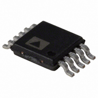
AD7992BRMZ-1 Analog Devices Inc, AD7992BRMZ-1 Datasheet - Page 16

AD7992BRMZ-1
Manufacturer Part Number
AD7992BRMZ-1
Description
IC ADC 12BIT 2CHAN I2C 10-MSOP
Manufacturer
Analog Devices Inc
Datasheet
1.AD7992BRMZ-1.pdf
(28 pages)
Specifications of AD7992BRMZ-1
Data Interface
I²C, Serial
Operating Temperature
-40°C ~ 125°C
Number Of Bits
12
Sampling Rate (per Second)
79k
Number Of Converters
1
Power Dissipation (max)
2.2mW
Voltage Supply Source
Single Supply
Mounting Type
Surface Mount
Package / Case
10-TFSOP (0.118", 3.00mm Width)
Resolution (bits)
12bit
Input Channel Type
Single Ended
Supply Voltage Range - Analogue
2.7V To 5.5V
Supply Current
1.4mA
No. Of Pins
10
Sampling Rate
188kSPS
Rohs Compliant
Yes
Lead Free Status / RoHS Status
Lead free / RoHS Compliant
For Use With
EVAL-AD7992CB - BOARD EVALUATION FOR AD7992
Lead Free Status / RoHS Status
Lead free / RoHS Compliant
Available stocks
Company
Part Number
Manufacturer
Quantity
Price
Part Number:
AD7992BRMZ-1
Manufacturer:
ADI/亚德诺
Quantity:
20 000
AD7992
INTERNAL REGISTER STRUCTURE
The AD7992 contains 11 internal registers (see Figure 24) that
are used to store conversion results, high and low conversion
limits, and information to configure and control the device.
There are ten data registers and one address pointer register.
Each data register has an address that the address pointer
register points to when communicating with it. The conversion
result register is the only data register that is read-only.
REGISTER
ADDRESS
POINTER
SERIAL BUS INTERFACE
Figure 24. AD7992 Register Structure
RESULT REGISTER
CONFIGURATION
ALERT STATUS
REGISTER CH1
REGISTER CH1
REGISTER CH1
REGISTER CH2
REGISTER CH2
REGISTER CH2
CONVERSION
CYCLE TIMER
HYSTERESIS
HYSTERESIS
REGISTER
REGISTER
REGISTER
DATA
DATA
DATA
DATA
LOW
HIGH
HIGH
LOW
D
A
A
T
SDA
SCL
Rev. 0 | Page 16 of 28
ADDRESS POINTER REGISTER
Because it is the register to which the first data byte of every
write operation is written automatically, the address pointer
register does not have and does not require an address. The
address pointer register is an 8-bit register in which the 4 LSBs
are used as pointer bits to store an address that points to one of
the AD7992’s data registers. The 4 MSBs are used as command
bits when operating in Mode 2 (see the Modes of Operation
section). The first byte following each write address is the
address of one of the data registers, which is stored in the
address pointer register and selects the data register to which
subsequent data bytes are written. Only the 4 LSBs of this
register are used to select a data register. On power-up, the
address pointer register contains all 0s, pointing to the
conversion result register.
Table 7. Address Pointer Register
C4
0
Table 8. AD7992 Register Addresses
P3
0
0
0
0
0
0
0
0
1
1
P2
0
0
0
0
1
1
1
1
0
0
C3
0
P1
0
0
1
1
0
0
1
1
0
0
C2
0
P0
0
1
0
1
0
1
0
1
0
1
Registers
Conversion result register (read)
Alert status register (read/write)
Configuration register (read/write)
Cycle Timer register (read/write)
DATA
DATA
Hysteresis register CH1 (read/write)
DATA
DATA
Hysteresis register CH2 (read/write)
C1
0
LOW
HIGH
LOW
HIGH
P3
register CH1 (read/write)
register CH2 (read/write)
register CH1 (read/write)
register CH2 (read/write)
Register select
P2
P1
P0


