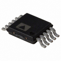
AD7992BRMZ-1 Analog Devices Inc, AD7992BRMZ-1 Datasheet - Page 13

AD7992BRMZ-1
Manufacturer Part Number
AD7992BRMZ-1
Description
IC ADC 12BIT 2CHAN I2C 10-MSOP
Manufacturer
Analog Devices Inc
Datasheet
1.AD7992BRMZ-1.pdf
(28 pages)
Specifications of AD7992BRMZ-1
Data Interface
I²C, Serial
Operating Temperature
-40°C ~ 125°C
Number Of Bits
12
Sampling Rate (per Second)
79k
Number Of Converters
1
Power Dissipation (max)
2.2mW
Voltage Supply Source
Single Supply
Mounting Type
Surface Mount
Package / Case
10-TFSOP (0.118", 3.00mm Width)
Resolution (bits)
12bit
Input Channel Type
Single Ended
Supply Voltage Range - Analogue
2.7V To 5.5V
Supply Current
1.4mA
No. Of Pins
10
Sampling Rate
188kSPS
Rohs Compliant
Yes
Lead Free Status / RoHS Status
Lead free / RoHS Compliant
For Use With
EVAL-AD7992CB - BOARD EVALUATION FOR AD7992
Lead Free Status / RoHS Status
Lead free / RoHS Compliant
Available stocks
Company
Part Number
Manufacturer
Quantity
Price
Part Number:
AD7992BRMZ-1
Manufacturer:
ADI/亚德诺
Quantity:
20 000
CIRCUIT INFORMATION
The AD7992 is a low power, 12-bit, single-supply, 2-channel
analog-to-digital converter (ADC). The part can be operated
from a 2.7 V to 5.5 V supply.
The AD7992 provides the user with a 2-channel multiplexer,
an on-chip track-and-hold, an ADC, an on-chip oscillator,
internal data registers, and an I
all housed in a 10-lead MSOP package that offers the user
considerable space-saving advantages over alternative solutions.
The AD7992 requires an external reference in the range of 1.2 V
to V
The AD7992 normally remains in a power-down state while not
converting. When supplies are first applied, the part comes up
in a power-down state. Power-up is initiated prior to a con-
version, and the device returns to power-down upon
completion of the conversion. Conversions can be initiated on
the AD7992 by pulsing the CONVST signal, using an automatic
cycle interval mode or a command mode where wake-up and a
conversion occur during a write address function (see the
Modes of Operation section). On completion of a conversion,
the AD7992 again enters power-down mode. This automatic
power-down feature allows power saving between conversions.
This means any read or write operations across the I
can occur while the device is in power-down.
CONVERTER OPERATION
The AD7992 is a successive approximation, analog-to-digital
converter based around a capacitive DAC. Figure 17 and
Figure 18 show simplified schematics of the ADC during its
acquisition and conversion phases, respectively. Figure 17 shows
the ADC during its acquisition phase. SW2 is closed and SW1 is
in position A, the comparator is held in a balanced condition,
and the sampling capacitor acquires the signal on V
AGND
V
IN
DD
.
A
SW1
B
Figure 17. ADC Acquisition Phase
SW2
2
C-compatible serial interface,
COMPARATOR
CAPACITIVE
IN
CONTROL
2
C interface
.
LOGIC
DAC
Rev. 0 | Page 13 of 28
When the ADC starts a conversion, as shown in Figure 18,
SW2 opens and SW1 moves to position B, causing the
comparator to become unbalanced. The input is disconnected
once the conversion begins. The control logic and the capacitive
DAC are used to add and subtract fixed amounts of charge from
the sampling capacitor to bring the comparator back into a
balanced condition. When the comparator is rebalanced, the
conversion is complete. The control logic generates the ADC
output code. Figure 19 shows the ADC transfer function.
ADC Transfer Function
The output coding of the AD7992 is straight binary. The
designed code transitions occur at successive integer LSB values
(i.e., 1 LSB, 2 LSB, and so on). The LSB size for the AD7992 is
REF
the AD7992.
AGND
V
IN
IN
/4096. Figure 19 shows the ideal transfer characteristic for
111...111
111...110
111...000
011...111
000...010
000...001
000...000
SW1
A
Figure 19. AD7992 Transfer Characteristic
B
Figure 18. ADC Conversion Phase
AGND + 1LSB
SW2
ANALOG INPUT
0V TO REF
AD7992 1LSB = REF
IN
COMPARATOR
+REF
IN
– 1LSB
IN
CAPACITIVE
/4096
CONTROL
LOGIC
AD7992
DAC


