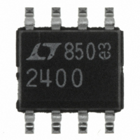
LTC2400CS8#PBF Linear Technology, LTC2400CS8#PBF Datasheet - Page 21

LTC2400CS8#PBF
Manufacturer Part Number
LTC2400CS8#PBF
Description
IC A/D CONV 24BIT MICRPWR 8-SOIC
Manufacturer
Linear Technology
Datasheet
1.LTC2400CS8PBF.pdf
(40 pages)
Specifications of LTC2400CS8#PBF
Number Of Bits
24
Sampling Rate (per Second)
7.5
Data Interface
MICROWIRE™, Serial, SPI™
Number Of Converters
1
Power Dissipation (max)
1mW
Voltage Supply Source
Single Supply
Operating Temperature
0°C ~ 70°C
Mounting Type
Surface Mount
Package / Case
8-SOIC (0.154", 3.90mm Width)
Lead Free Status / RoHS Status
Lead free / RoHS Compliant
Available stocks
Company
Part Number
Manufacturer
Quantity
Price
APPLICATIONS
Figure 14. CS Capacitance vs Supply Current
300
250
200
150
100
Figure 13. CS Capacitance vs Output Rate
50
7
6
5
4
3
2
1
0
8
7
6
5
4
3
2
0
0
1
Figure 12. CS Capacitance vs t
1
0
1
10
10
10
U
CAPACITANCE ON CS (pF)
CAPACITANCE ON CS (pF)
CAPACITANCE ON CS (pF)
V
V
CC
CC
V
= 5V
= 3V
CC
100
100
100
INFORMATION
= 5V
U
1000
1000
1000
V
CC
V
= 5V
CC
10000
10000
W
10000
= 3V
V
CC
SAMPLE
2400 F12
= 3V
2400 F13
2400 F14
100000
100000
100000
U
pin on each falling edge of SCK. The internally generated
serial clock is output to the SCK pin. This signal may be
used to shift the conversion result into external circuitry.
After the 32nd rising edge, CS is pulled HIGH and a new
conversion is immediately started. This is useful in appli-
cations requiring periodic monitoring and ultralow power.
Figure 14 shows the average supply current as a function
of capacitance on CS.
It should be noticed that the external capacitor discharge
current is kept very small in order to decrease the con-
verter power dissipation in the sleep state. In the autostart
mode the analog voltage on the CS pin cannot be observed
without disturbing the converter operation using a regular
oscilloscope probe. When using this configuration, it is
important to minimize the external leakage current at the
CS pin by using a low leakage external capacitor and
properly cleaning the PCB surface.
The internal serial clock mode is selected every time the
voltage on the CS pin crosses an internal threshold volt-
age. An internal weak pull-up at the SCK pin is active while
CS is discharging; therefore, the internal serial clock
timing mode is automatically selected if SCK is floating. It
is important to ensure there are no external drivers pulling
SCK LOW while CS is discharging.
DIGITAL SIGNAL LEVELS
The LTC2400’s digital interface is easy to use. Its digital
inputs (F
accept standard TTL/CMOS logic levels and the internal
hysteresis receivers can tolerate edge rates as slow as
100 s. However, some considerations are required to take
advantage of exceptional accuracy and low supply current.
The digital output signals (SDO and SCK in Internal SCK
mode of operation) are less of a concern because they are
not generally active during the conversion state.
In order to preserve the LTC2400’s accuracy, it is very
important to minimize the ground path impedance which
may appear in series with the input and/or reference signal
and to reduce the current which may flow through this
path. The GND pin should be connected to a low resistance
ground plane through a minimum length trace. The use of
multiple via holes is recommended to further reduce the
O
, CS and SCK in External SCK mode of operation)
LTC2400
21


