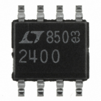
LTC2400CS8#PBF Linear Technology, LTC2400CS8#PBF Datasheet - Page 16

LTC2400CS8#PBF
Manufacturer Part Number
LTC2400CS8#PBF
Description
IC A/D CONV 24BIT MICRPWR 8-SOIC
Manufacturer
Linear Technology
Datasheet
1.LTC2400CS8PBF.pdf
(40 pages)
Specifications of LTC2400CS8#PBF
Number Of Bits
24
Sampling Rate (per Second)
7.5
Data Interface
MICROWIRE™, Serial, SPI™
Number Of Converters
1
Power Dissipation (max)
1mW
Voltage Supply Source
Single Supply
Operating Temperature
0°C ~ 70°C
Mounting Type
Surface Mount
Package / Case
8-SOIC (0.154", 3.90mm Width)
Lead Free Status / RoHS Status
Lead free / RoHS Compliant
Available stocks
Company
Part Number
Manufacturer
Quantity
Price
APPLICATIONS
LTC2400
External Serial Clock, 2-Wire I/O
This timing mode utilizes a 2-wire serial I/O interface. The
conversion result is shifted out of the device by an exter-
nally generated serial clock (SCK) signal, see Figure 7. CS
may be permanently tied to ground (Pin 4), simplifying the
user interface or isolation barrier.
The external serial clock mode is selected at the end of the
power-on reset (POR) cycle. The POR cycle is concluded
approximately 0.5ms after V
applied to SCK at this time determines if SCK is internal or
external. SCK must be driven LOW prior to the end of POR
in order to enter the external serial clock timing mode.
Since CS is tied LOW, the end-of-conversion (EOC) can be
continuously monitored at the SDO pin during the convert
and sleep states. EOC may be used as an interrupt to an
external controller indicating the conversion result is
ready. EOC = 1 while the conversion is in progress and EOC
= 0 once the conversion enters the low power sleep state.
On the falling edge of EOC, the conversion result is loaded
into an internal static shift register. The device remains in
the sleep state until the first rising edge of SCK. Data is
16
(EXTERNAL)
SDO
SCK
CS
SLEEP
U
BIT 0
EOC
INFORMATION
U
CONVERSION
Hi-Z
CC
DATA OUTPUT
TEST EOC
Figure 6. External Serial Clock, Reduced Data Output Length
exceeds 2.2V. The level
W
Hi-Z
TEST EOC
–0.12V
SLEEP
Hi-Z
REF
U
TO 1.12V
0.1V TO V
BIT 31
EOC
1 F
2.7V TO 5.5V
V
REF
V
REF
CC
IN
BIT 30
V
V
V
GND
CC
REF
IN
LTC2400
shifted out the SDO pin on each falling edge of SCK
enabling external circuitry to latch data on the rising edge
of SCK. EOC can be latched on the first rising edge of SCK.
On the 32nd falling edge of SCK, SDO goes HIGH (EOC =
1) indicating a new conversion has begun.
Internal Serial Clock, Single Cycle Operation
This timing mode uses an internal serial clock to shift out
the conversion result and a CS signal to monitor and
control the state of the conversion cycle, see Figure 8.
In order to select the internal serial clock timing mode, the
serial clock pin (SCK) must be floating (HI-Z) or pulled
HIGH prior to the falling edge of CS. The device will not
enter the internal serial clock mode if SCK is driven LOW
on the falling edge of CS. An internal weak pull-up resistor
is active on the SCK pin during the falling edge of CS;
therefore, the internal serial clock timing mode is auto-
matically selected if SCK is not externally driven.
The serial data output pin (SDO) is HI-Z as long as CS is
HIGH. At any time during the conversion cycle, CS may be
pulled LOW in order to monitor the state of the converter.
BIT 29
SDO
SIG
SCK
CS
F
O
DATA OUTPUT
BIT 28
EXR
V
CC
BIT 27
= 50Hz REJECTION
= EXTERNAL OSCILLATOR
= 60Hz REJECTION
MSB
BIT 9
BIT 8
Hi-Z
CONVERSION
TEST EOC
2400 F06


