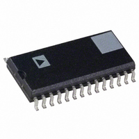
AD73322LAR Analog Devices Inc, AD73322LAR Datasheet - Page 12

AD73322LAR
Manufacturer Part Number
AD73322LAR
Description
IC ANALOG FRONT END DUAL 28-SOIC
Manufacturer
Analog Devices Inc
Datasheet
1.AD73322LARZ.pdf
(48 pages)
Specifications of AD73322LAR
Rohs Status
RoHS non-compliant
Number Of Bits
16
Number Of Channels
4
Power (watts)
73mW
Voltage - Supply, Analog
2.7 V ~ 5.5 V
Voltage - Supply, Digital
2.7 V ~ 5.5 V
Package / Case
28-SOIC (7.5mm Width)
Available stocks
Company
Part Number
Manufacturer
Quantity
Price
Company:
Part Number:
AD73322LARU
Manufacturer:
LINEA
Quantity:
5
Company:
Part Number:
AD73322LARUZ
Manufacturer:
AD
Quantity:
760
Part Number:
AD73322LARUZ
Manufacturer:
ADI/亚德诺
Quantity:
20 000
AD73322L
TERMINOLOGY
Absolute Gain
A measure of converter gain for a known signal. Absolute gain
is measured (differentially) with a 1 kHz sine wave at 0 dBm0
for the DAC and with a 1 kHz sine wave at 0 dBm0 for the
ADC. The absolute gain specification is used for gain tracking
error specification.
Crosstalk
Crosstalk is due to coupling of signals from a given channel to
an adjacent channel. It is defined as the ratio of the amplitude
of the coupled signal to the amplitude of the input signal.
Crosstalk is expressed in dB.
Gain Tracking Error
Measures changes in converter output for different signal levels
relative to an absolute signal level. The absolute signal level is
0 dBm0 (equal to absolute gain) at 1 kHz for the DAC and 0
dBm0 (equal to absolute gain) at 1 kHz for the ADC. Gain
tracking error at 0 dBm0 (ADC) and 0 dBm0 (DAC) is 0 dB
by definition.
Group Delay
The derivative of radian phase with respect to radian frequency,
dø(f)/df. Group delay is a measure of the average delay of a
system as a function of frequency. A linear system with a
constant group delay has a linear phase response. The deviation
of group delay from a constant indicates the degree of nonlinear
phase response of the system.
Idle Channel Noise
The total signal energy measured at the output of the device
when the input is grounded (measured in the frequency range
300 Hz to 3400 Hz).
Intermodulation Distortion
With inputs consisting of sine waves at two frequencies, fa and
fb, any active device with nonlinearities creates distortion
products at sum and difference frequencies of mfa ± nfb where
m, n = 0, 1, 2, 3, etc. Intermodulation terms are those for which
neither m nor n is equal to zero. For final testing, the second-
order terms include (fa + fb) and (fa − fb), while the third-order
terms include (2fa + fb), (2fa − fb), (fa + 2fb) and (fa − 2fb).
Power Supply Rejection
Measures the susceptibility of a device to noise on the power
supply. Power supply rejection is measured by modulating the
power supply with a sine wave and measuring the noise at the
output (relative to 0 dB).
Rev. A | Page 12 of 48
Sample Rate
The rate at which the ADC updates its output register and the
DAC updates its output from its input register. The sample rate
can be chosen from a list of four that are fixed relative to the
DMCLK. Sample rate is set by programming bits DIR0-1 in
Control Register B of each channel.
SNR + THD
Signal-to-noise ratio plus harmonic distortion is the ratio of the
rms value of the measured input signal to the rms sum of all
other spectral components in the frequency range 300 Hz to
3400 Hz, including harmonics but excluding dc.
ABBREVIATIONS
Table 7.
Abbreviation
ADC
AFE
AGT
ALB
BW
CRx
CRx:n
DAC
DGT
DLB
DMCLK
FS
FSLB
PGA
SC
SLB
SNR
SPORT
THD
VBW
Definition
Analog-to-digital converter.
Analog front end.
Analog gain tap.
Analog loop-back.
Bandwidth.
A control register where x is a placeholder for
an alphabetic character (A to H). There are eight
read/write control registers on the AD73322L—
CRA through CRH.
A bit position, where n is a placeholder for a
numeric character (0 to 7), within a control
register, where x is a placeholder for an
alphabetic character (A to E). Position 7
represents the MSB and Position 0 represents
the LSB.
Digital-to-analog converter.
Digital gain tap.
Digital loop-back.
Device (internal) master clock. This is the
internal master clock resulting from the
external master clock (MCLK) being divided by
the on-chip master clock divider.
Full scale.
Frame sync loop-back—where the SDOFS of
the final device in a cascade is connected to the
RFS and TFS of the DSP and the SDIFS of first
device in the cascade. Data input and output
occur simultaneously. In the case of nonFSLB,
SDOFS and SDO are connected to the Rx port of
the DSP while SDIFS and SDI are connected to
the Tx port.
Programmable gain amplifier.
Switched capacitor.
SPORT loop-back.
Signal-to-noise ratio.
Serial port.
Total harmonic distortion.
Voice bandwidth.


