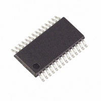
MAXQ3181-RAN+ Maxim Integrated Products, MAXQ3181-RAN+ Datasheet - Page 66

MAXQ3181-RAN+
Manufacturer Part Number
MAXQ3181-RAN+
Description
IC AFE POLYPHASE LO-PWR 28-TSSOP
Manufacturer
Maxim Integrated Products
Datasheet
1.MAXQ3181-RAN.pdf
(84 pages)
Specifications of MAXQ3181-RAN+
Number Of Channels
8
Power (watts)
35mW
Voltage - Supply, Analog
3.3V
Voltage - Supply, Digital
3.3V
Package / Case
28-TSSOP
Lead Free Status / RoHS Status
Lead free / RoHS Compliant
Number Of Bits
-
- Current page: 66 of 84
- Download datasheet (899Kb)
Low-Power, Active Energy, Polyphase AFE
These registers configure the time slot normally assigned to voltage channels A/B/C. The user may wish to change the
PGG settings to match the voltage sensor. However, it is recommended that the user not modify the ADCMX settings.
66
Bit:
Name:
Reset A:
Reset B:
Reset C:
BIT
7:4
2:0
______________________________________________________________________________________
3
DADCNV ADC Disable. When set, disables the ADC for this time slot.
ADCMX
NAME
PGG
7
Analog Input Select. This four-bit field determines which of the following analog inputs are sampled during
this time slot.
0000 = V0P - VN (Phase A Voltage: 0000)
0001 = V1P - VN (Phase B Voltage: 0001)
0010 = V2P - VN (Phase C Voltage: 0010)
0011 = I0P - I0N
0100 = I1P - I1N
0101 = I2P - I2N
0110 = INP - VN
1xxx = Temperature
Programmable Gain Amplifier Select. This three-bit field configures the programmable-gain amplifier at
the front-end of the analog input. The field has the following values:
000 = Gain of 1
001 = Gain of 2
010 = Gain of 4
011 = Gain of 8
100 = Gain of 16
101 = Gain of 32
All other values are reserved and can cause unpredictable behavior if selected.
6
ADCMX
Time Slot Assignment—Voltage Channel X = A/B/C (SCAN_VX)
0x0
0x1
0x2
5
4
FUNCTION
DADCNV
3
0
0
0
(A: 0x009, B: 0x00D, C: 0x00B)
2
PGG
0x0
0x0
0x0
1
0
Related parts for MAXQ3181-RAN+
Image
Part Number
Description
Manufacturer
Datasheet
Request
R

Part Number:
Description:
MAX7528KCWPMaxim Integrated Products [CMOS Dual 8-Bit Buffered Multiplying DACs]
Manufacturer:
Maxim Integrated Products
Datasheet:

Part Number:
Description:
Single +5V, fully integrated, 1.25Gbps laser diode driver.
Manufacturer:
Maxim Integrated Products
Datasheet:

Part Number:
Description:
Single +5V, fully integrated, 155Mbps laser diode driver.
Manufacturer:
Maxim Integrated Products
Datasheet:

Part Number:
Description:
VRD11/VRD10, K8 Rev F 2/3/4-Phase PWM Controllers with Integrated Dual MOSFET Drivers
Manufacturer:
Maxim Integrated Products
Datasheet:

Part Number:
Description:
Highly Integrated Level 2 SMBus Battery Chargers
Manufacturer:
Maxim Integrated Products
Datasheet:

Part Number:
Description:
Current Monitor and Accumulator with Integrated Sense Resistor; ; Temperature Range: -40°C to +85°C
Manufacturer:
Maxim Integrated Products

Part Number:
Description:
TSSOP 14/A�/RS-485 Transceivers with Integrated 100O/120O Termination Resis
Manufacturer:
Maxim Integrated Products

Part Number:
Description:
TSSOP 14/A�/RS-485 Transceivers with Integrated 100O/120O Termination Resis
Manufacturer:
Maxim Integrated Products

Part Number:
Description:
QFN 16/A�/AC-DC and DC-DC Peak-Current-Mode Converters with Integrated Step
Manufacturer:
Maxim Integrated Products

Part Number:
Description:
TDFN/A/65V, 1A, 600KHZ, SYNCHRONOUS STEP-DOWN REGULATOR WITH INTEGRATED SWI
Manufacturer:
Maxim Integrated Products

Part Number:
Description:
Integrated Temperature Controller f
Manufacturer:
Maxim Integrated Products

Part Number:
Description:
SOT23-6/I�/45MHz to 650MHz, Integrated IF VCOs with Differential Output
Manufacturer:
Maxim Integrated Products

Part Number:
Description:
SOT23-6/I�/45MHz to 650MHz, Integrated IF VCOs with Differential Output
Manufacturer:
Maxim Integrated Products

Part Number:
Description:
EVALUATION KIT/2.4GHZ TO 2.5GHZ 802.11G/B RF TRANSCEIVER WITH INTEGRATED PA
Manufacturer:
Maxim Integrated Products

Part Number:
Description:
QFN/E/DUAL PCIE/SATA HIGH SPEED SWITCH WITH INTEGRATED BIAS RESISTOR
Manufacturer:
Maxim Integrated Products
Datasheet:


