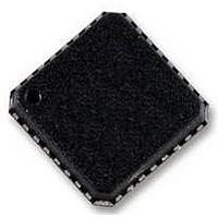
AD7195BCPZ Analog Devices Inc, AD7195BCPZ Datasheet - Page 37

AD7195BCPZ
Manufacturer Part Number
AD7195BCPZ
Description
IC AFE 24BIT 4.8K 32LFSP
Manufacturer
Analog Devices Inc
Datasheet
1.AD7195BCPZ-RL.pdf
(44 pages)
Specifications of AD7195BCPZ
Design Resources
Precision Weigh Scale Design Using AD7195 with Internal PGA and AC Excitation (CN0155)
Number Of Bits
24
Number Of Channels
4
Voltage - Supply, Analog
4.75 V ~ 5.25 V
Voltage - Supply, Digital
2.7 V ~ 5.25 V
Package / Case
32-LFCSP
Resolution (bits)
24bit
Sampling Rate
4.8kSPS
Input Channel Type
Pseudo Differential
Data Interface
3-Wire, Serial
Supply Voltage Range - Analog
4.75V To 5.25V
Lead Free Status / RoHS Status
Lead free / RoHS Compliant
Power (watts)
-
Lead Free Status / RoHS Status
Lead free / RoHS Compliant, Lead free / RoHS Compliant
Available stocks
Company
Part Number
Manufacturer
Quantity
Price
Company:
Part Number:
AD7195BCPZ
Manufacturer:
Analog Devices Inc
Quantity:
135
Company:
Part Number:
AD7195BCPZ
Manufacturer:
TST
Quantity:
5 000
Part Number:
AD7195BCPZ
Manufacturer:
ADI/亚德诺
Quantity:
20 000
Company:
Part Number:
AD7195BCPZ-RL
Manufacturer:
SEMTECH
Quantity:
394
The output data rate equals
where:
f
f
FS[9:0] is the decimal equivalent of Bit FS9 to Bit FS0 in the
mode register.
When the analog input is constant or a channel change occurs,
valid conversions are available at a constant output data rate.
When conversions are being performed on a single channel and
a step change occurs on the analog input, the ADC continues to
output fully settled conversions if the step change is synchronized
with the conversion process. If the step change is asynchronous,
one conversion is output from the ADC that is not completely
settled (see Figure 35).
Table 32 provides examples of output data rates and the corres-
ponding FS values.
Table 32. Examples of Output Data Rates and the
Corresponding Settling Time (Zero Latency)
FS[9:0]
480
96
80
ADC
CLK
is the master clock (4.92 MHz nominal).
is the output data rate.
f
ANALOG
OUTPUT
ADC
INPUT
ADC
= 1/t
Output Data Rate (Hz)
3.3
16.7
20
SETTLE
Figure 35. Sinc
= f
CLK
/(3 × 1024 × FS[9:0])
3
Zero Latency Operation
1/
f
ADC
Settling Time (ms)
300
60
50
SETTLED
FULLY
Rev. 0 | Page 37 of 44
Sinc
Figure 36 show the frequency response of the sinc
FS[9:0] is set to 96 and the master clock equals 4.92 MHz. The
output data rate is equal to 50 Hz when zero latency is disabled
and 16.7 Hz when zero latency is enabled. The sinc
50 Hz ± 1 Hz rejection of 95 dB minimum for a stable master clock.
When FS[9:0] is set to 80 and the master clock equals
4.92 MHz, 60 Hz rejection is achieved (see Figure 37). The
output data rate is equal to 60 Hz when zero latency is disabled
and 20 Hz when zero latency is enabled. The sinc
rejection of 95 dB minimum at 60 Hz ± 1 Hz, assuming a stable
master clock.
3
–100
–120
–100
–120
–110
–110
50 Hz/60 Hz Rejection
–10
–20
–30
–40
–50
–60
–70
–80
–90
–10
–20
–30
–40
–50
–60
–70
–80
–90
0
0
0
0
Figure 36. Sinc
Figure 37. Sinc
25
30
50
3
3
FREQUENCY (Hz)
FREQUENCY (Hz)
Filter Response (FS[9:0] = 96)
Filter Response (FS[9:0] = 80)
60
75
90
100
120
125
3
3
filter has
3
filter when
AD7195
filter gives
150
150


