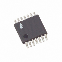
ISL12028IV27Z-T Intersil, ISL12028IV27Z-T Datasheet - Page 6

ISL12028IV27Z-T
Manufacturer Part Number
ISL12028IV27Z-T
Description
IC RTC EEPROM LP 14-TSSOP
Manufacturer
Intersil
Type
Clock/Calendar/Supervisor/EEPROMr
Datasheet
1.ISL12028IV27Z-T.pdf
(29 pages)
Specifications of ISL12028IV27Z-T
Memory Size
4K (512 x 8)
Time Format
HH:MM:SS (12/24 hr)
Date Format
YY-MM-DD-dd
Interface
I²C, 2-Wire Serial
Voltage - Supply
2.7 V ~ 5.5 V
Operating Temperature
-40°C ~ 85°C
Mounting Type
Surface Mount
Package / Case
14-TSSOP
Rohs Compliant
YES
Lead Free Status / RoHS Status
Lead free / RoHS Compliant
Other names
ISL12028IV27Z-TTR
Available stocks
Company
Part Number
Manufacturer
Quantity
Price
Company:
Part Number:
ISL12028IV27Z-T
Manufacturer:
Intersil
Quantity:
2 500
Company:
Part Number:
ISL12028IV27Z-T
Manufacturer:
Intersil
Quantity:
39 253
Serial Interface (I
NOTES:
10. Bit BSW = 0 (Standard Mode), ATR = 00h, V
12. In order to ensure proper timekeeping, the V
13. Parameter is not 100% tested.
14. t
15. These are I
16. Compliance to datasheet limits is assured by one or more methods: production test, characterization and/or design.
11. Specified at +25°C.
7. IRQ/F
8. V
9. V
SYMBOL
t
t
t
t
t
t
HD:STA
SU:DAT
HD:DAT
SU:STO
HD:STO
SU:STA
t
t
Cpin
t
R
HIGH
sequence of a serial interface Write operation, to the end of the self-timed internal non-volatile write cycle.
LOW
t
t
t
BUF
WC
Cb
Cb
WC
AA
DH
t
t
IL
RESET
PU
R
F
= V
is the minimum cycle time to be allowed for any non-volatile Write by the user, it is the time from valid STOP condition at the end of Write
OUT
DD
= 2.63V (V
SCL Falling Edge to SDA Output
Data Valid
Time the bus must be free before
the start of a new transmission
Clock LOW Time
Clock HIGH Time
START Condition Setup Time
START Condition Hold Time
Input Data Setup Time
Input Data Hold Time
STOP Condition Setup Time
STOP Condition Hold Time for
Read, or Volatile Only Write
Output Data Hold Time
Capacitive Loading of SDA or SCL Total on-chip and off-chip
SDA, and SCL Pin Capacitance
Non-volatile Write Cycle Time
SDA and SCL Rise Time
SDA and SCL Fall Time
Capacitive Loading of SDA or SCL Total on-chip and off-chip
SDA and SCL Bus Pull-up Resistor
Off-chip
x 0.1, V
Inactive (no frequency output and no alarms).
2
C specific parameters and are not directly tested, however they are used during device testing to validate device specification.
IH
2
DD
C) Specifications
PARAMETER
= V
must be greater than V
DD
x 0.9, f
6
SCL
= 400kHz.
Boldface limits apply over the operating temperature range, -40°C to +85°C. (Continued)
BAT
DD SR-
RESET
SCL falling edge crossing 30% of V
until SDA exits the 30% to 70% of V
window.
SDA crossing 70% of V
STOP condition, to SDA crossing 70%
of V
condition.
Measured at the 30% of V
Measured at the 70% of V
SCL rising edge to SDA falling edge.
Both crossing 70% of V
From SDA falling edge crossing 30%
of V
70% of V
From SDA exiting the 30% to 70% of
V
crossing 30% of V
From SCL falling edge crossing 70%
of V
70% of V
From SCL rising edge crossing 70% of
V
of V
From SDA rising edge to SCL falling
edge. Both crossing 70% of V
From SCL falling edge crossing 30%
of V
70% of V
From 30% to 70% of V
From 70% to 30% of V
Maximum is determined by t
For Cb = 400pF, max is about
2kΩ~2.5kΩ.
For Cb = 40pF, max is about
15kΩ~20kΩ
DD
DD
≥ 1.8V.
DD
DD
DD
DD
DD
, to SDA rising edge crossing 30%
window, to SCL rising edge
specification must be followed.
), V
ISL12028, ISL12028A
.
, until SDA enters the 30% to
during the following START
to SCL falling edge crossing
to SDA entering the 30% to
DD
DD
DD
BAT
CONDITIONS
.
window.
window.
= 0V.
DD
DD
DD
DD
DD
DD
DD
.
during a
R
crossing.
crossing.
DD
and t
.
DD
DD
F
.
,
20 + 0.1 x Cb
20 + 0.1 x Cb
(Note 16)
1300
1300
MIN
600
600
600
100
600
600
10
10
0
0
1
TYP
12
(Note 16)
MAX
900
400
250
250
400
10
20
UNITS
ms
kΩ
ns
ns
ns
ns
ns
ns
ns
ns
ns
ns
ns
pF
pF
ns
ns
pF
November 30, 2010
NOTES
FN8233.9
14
15
15
15
15


