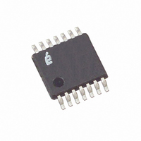
ISL12028IV27Z-T Intersil, ISL12028IV27Z-T Datasheet - Page 14

ISL12028IV27Z-T
Manufacturer Part Number
ISL12028IV27Z-T
Description
IC RTC EEPROM LP 14-TSSOP
Manufacturer
Intersil
Type
Clock/Calendar/Supervisor/EEPROMr
Datasheet
1.ISL12028IV27Z-T.pdf
(29 pages)
Specifications of ISL12028IV27Z-T
Memory Size
4K (512 x 8)
Time Format
HH:MM:SS (12/24 hr)
Date Format
YY-MM-DD-dd
Interface
I²C, 2-Wire Serial
Voltage - Supply
2.7 V ~ 5.5 V
Operating Temperature
-40°C ~ 85°C
Mounting Type
Surface Mount
Package / Case
14-TSSOP
Rohs Compliant
YES
Lead Free Status / RoHS Status
Lead free / RoHS Compliant
Other names
ISL12028IV27Z-TTR
Available stocks
Company
Part Number
Manufacturer
Quantity
Price
Company:
Part Number:
ISL12028IV27Z-T
Manufacturer:
Intersil
Quantity:
2 500
Company:
Part Number:
ISL12028IV27Z-T
Manufacturer:
Intersil
Quantity:
39 253
The effective series load capacitance is the combination of
C
For example, C
(ATR = 100000) = 4.5pF, and C
The entire range for the series combination of load capacitance
goes from 4.5pF to 20.25pF in 0.25pF steps. Note that these
are typical values.
DTR Register - DTR2, DTR1, DTR0: Digital
Trimming Register
The digital trimming Bits DTR2, DTR1 and DTR0 adjust the
number of counts per second and average the ppm error to
achieve better accuracy.
DTR2 is a sign bit. DTR2 = 0 means frequency
compensation is > 0. DTR2 = 1 means frequency
compensation is < 0.
DTR1 and DTR0 are scale bits. DTR1 gives 10ppm
adjustment and DTR0 gives 20ppm adjustment.
A range from -30ppm to +30ppm can be represented by
using the three DTR bits.
PWR Register: SBIB, BSW, VTS2, VTS1, VTS0
SBIB: - Serial Bus Interface (Enable)
The serial bus can be disabled in battery backup mode by
setting this bit to “1”. This will minimize power drain on the
battery. The Serial Interface can be enabled in battery
backup mode by setting this bit to “0”. (default is “0”). See
“RESET” on page 9 and “Power Control Operation” on
page 15.
BSW: Power Control Bit
The Power Control bit, BSW, determines the conditions for
switching between V
options.
C
C
X1
LOAD
LOAD
DTR2
and C
0
0
0
0
1
1
1
1
=
=
DTR REGISTER
⎛
⎝
---------------------------------- -
⎛
⎝
TABLE 5. DIGITAL TRIMMING REGISTERS
X2
---------- -
C
16 b5
---------------------------------------------------------------------------------------------------------------------------- -
1
X1
⋅
DTR1
as shown in Equation 2:
LOAD
1
+
0
1
0
1
0
1
0
1
---------- -
C
+
1
8 b4
X2
⋅
(ATR = 00000) = 12.5pF, C
⎞
⎠
DD
+
and Back Up Battery. There are two
DTR0
4 b3
⋅
0
0
1
1
0
0
1
1
14
+
LOAD
2 b2
2
⋅
ESTIMATED FREQUENCY
(ATR = 011111) = 20.25pF.
+
1 b1
⋅
+
0.5 b0
PPM
+10
+20
+30
-10
-20
-30
LOAD
0
0
⋅
ISL12028, ISL12028A
+
9
⎞ pF
⎠
(EQ. 2)
ISL12028A)
ISL12028)
See “Power Control Operation” on page 15 for more details.
Also see “I
LVR Operation” in the “Application Section” on page 22 for
important details.
VTS2, VTS1, VTS0: V
The ISL12028 is shipped with a default V
(V
This register is a non-volatile with no protection, therefore
any writes to this location can change the default value from
that marked on the package. If not changed with a
non-volatile write, this value will not change over normal
operating and storage conditions. However, ISL12028 has
four (4) additional selectable levels to fit the customers
application. Levels are: 4.64V(default), 4.38V, 3.09V, 2.92V
and 2.63V. The V
and VTS0) (see Table 6).
Care should be taken when changing the V
If the V
device will go into RESET and unless V
device will no longer be able to communicate using the I
In battery mode, the RESET signal output is asserted LOW
when the V
threshold, but the RESET signal output will not return HIGH
until the device is back to V
above V
Device Operation
Writing to the Clock/Control Registers
Changing any of the bits of the clock/control registers
requires the following steps:
1. Write a 02h to the Status Register to set the Write Enable
2. Write a 06h to the Status Register to set both the Register
Option 1 Standard Mode: Set “BSW = 0” (default for
Option 2 Legacy/Default Mode: Set “BSW = 1” (default for
RESET
VTS2
Latch (WEL). This is a volatile operation, so there is no
delay after the write. (Operation preceded by a start and
ended with a stop).
Write Enable Latch (RWEL) and the WEL bit. This is also
a volatile cycle. The zeros in the data byte are required.
(Operation proceeded by a start and ended with a stop).
0
0
0
0
1
RESET
RESET
) per the “Ordering Information” table on page 2.
2
DD
C Communications During Battery backup and
VTS1
voltage selected is higher than V
voltage supply has dipped below the V
threshold.
TABLE 6. V
0
0
1
1
0
RESET
selection is via 3 bits (VTS2, VTS1
RESET
VTS0
RESET
0
1
0
1
0
DD
mode even the V
Select Bits
SELECTION
DD
DD
V
RESET
RESET
is increased, the
4.64
4.38
3.09
2.92
2.63
threshold
November 30, 2010
DD
DD
(V)
select bits.
, then the
voltage is
RESET
FN8233.9
2
C.


