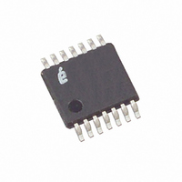
ISL12028IV27Z-T Intersil, ISL12028IV27Z-T Datasheet - Page 12

ISL12028IV27Z-T
Manufacturer Part Number
ISL12028IV27Z-T
Description
IC RTC EEPROM LP 14-TSSOP
Manufacturer
Intersil
Type
Clock/Calendar/Supervisor/EEPROMr
Datasheet
1.ISL12028IV27Z-T.pdf
(29 pages)
Specifications of ISL12028IV27Z-T
Memory Size
4K (512 x 8)
Time Format
HH:MM:SS (12/24 hr)
Date Format
YY-MM-DD-dd
Interface
I²C, 2-Wire Serial
Voltage - Supply
2.7 V ~ 5.5 V
Operating Temperature
-40°C ~ 85°C
Mounting Type
Surface Mount
Package / Case
14-TSSOP
Rohs Compliant
YES
Lead Free Status / RoHS Status
Lead free / RoHS Compliant
Other names
ISL12028IV27Z-TTR
Available stocks
Company
Part Number
Manufacturer
Quantity
Price
Company:
Part Number:
ISL12028IV27Z-T
Manufacturer:
Intersil
Quantity:
2 500
Company:
Part Number:
ISL12028IV27Z-T
Manufacturer:
Intersil
Quantity:
39 253
NOTE: Shaded cells indicate that NO other value is to be written to that bit. X indicates the bits are set according to the product variation, see device
“Ordering Information on page 2).
Unused Bits
Bit 3 in the SR is not used, but must be zero. The Data Byte
output during a SR read will contain a zero in this bit
location.
Alarm Registers (Non-Volatile)
Alarm0 and Alarm1
The alarm register bytes are set up identical to the RTC
register bytes, except that the MSB of each byte functions as
an enable bit (enable = “1”). These enable bits specify which
ADDR.
000D
000C
003F
0037
0036
0035
0034
0033
0032
0031
0030
0014
0013
0012
0010
000F
000E
000B
000A
0009
0008
0007
0006
0005
0004
0003
0002
0001
0000
0011
(EEPROM
(EEPROM
(EEPROM
(SRAM)
Control
Alarm1
Alarm0
Status
TYPE
RTC
)
)
)
NAME
DWA1
MOA1
MNA1
DWA0
MOA0
MNA0
YRA1
HRA1
YRA0
HRA0
DTA1
SCA1
DTA0
SCA0
PWR
Y2K1
Y2K0
REG
DTR
Y2K
ATR
DW
MO
INT
HR
MN
SR
YR
DT
SC
BL
EDW1
EMO1
EDW0
EMO0
12
EHR1
EMN1
EHR0
EMN0
EDT1
ESC1
EDT0
ESC0
SBIB
BAT
Y23
BP2
MIL
IM
0
0
0
0
0
0
0
0
0
0
7
Unused - Default = RTC Year value (No EEPROM) - Future expansion
Unused - Default = RTC Year value (No EEPROM) - Future expansion
A1M22
A0M22
A1S22
A0S22
AL1E
BSW
M22
AL1
Y22
S22
BP1
6
0
0
0
0
0
0
0
0
0
0
0
0
0
0
0
0
0
TABLE 2. CLOCK/CONTROL MEMORY MAP
A1Y2K21 A1Y2K20 A1Y2K13
A0Y2K21 A0Y2K20 A0Y2K13
A1M21
A0M21
Y2K21
A1D21
A1H21
A1S21
A0D21
A0H21
A0S21
ATR5
AL0E
M21
AL0
Y21
D21
H21
S21
BP0
ISL12028, ISL12028A
5
0
0
0
0
0
0
0
0
A1G20
A1M20
A0G20
A0M20
Y2K20
A1D20
A1H20
A1S20
A0D20
A0H20
A0S20
OSCF
ATR4
WD1
G20
M20
FO1
Y20
D20
H20
S20
4
0
0
0
0
0
BIT
A1G13
A1M13
A0G13
A0M13
Y2K13
A1D13
A1H13
A1S13
A0D13
A0H13
A0S13
ATR3
WD0
M13
FO0
Y13
G13
D13
H13
S13
alarm registers (seconds, minutes, etc.) are used to make
the comparison. Note that there is no alarm byte for year.
The alarm function works as a comparison between the
alarm registers and the RTC registers. As the RTC
advances, the alarm will be triggered once a match occurs
between the alarm registers and the RTC registers. Any one
alarm register, multiple registers, or all registers can be
enabled for a match. See “Device Operation” on page 14
and “Application Section” on page 22 for more information.
3
0
0
0
0
0
0
A1G12
A1M12
A0G12
A0M12
A1D12
A1H12
A1S12
A0D12
A0H12
A0S12
RWEL
VTS2
DTR2
ATR2
DY2
M12
DY2
DY2
Y12
G12
D12
H12
S12
2
0
0
0
0
0
A1G11
A1D11
A1H11
A1M11
A0G11
A0D11
A0H11
A0M11
A1S11
A0S11
DTR1
VTS1
ATR1
WEL
DY1
DY1
DY1
G11
M11
Y11
D11
H11
S11
1
0
0
0
0
0
A1Y2K10
A0Y2K10
A1M10
A0M10
A1G10
A1D10
A1H10
A1S10
A0G10
A0D10
A0H10
A0S10
Y2K10
RTCF
DTR0
VTS0
ATR0
DY0
G10
D10
H10
M10
DY0
DY0
Y10
S10
0
0
0
0 to 59
0 to 59
0 to 99
1 to 12
1 to 31
0 to 23
0 to 59
0 to 59
1 to 12
1 to 31
0 to 23
0 to 59
1 to 12
1 to 31
0 to 23
0 to 59
RANG
19/20
0 to 6
19/20
0 to 6
19/20
0 to 6
E
November 30, 2010
4Xh
01h
20h
00h
00h
00h
01h
00h
00h
00h
00h
00h
00h
18h
20h
00h
00h
00h
00h
00h
00h
20h
00h
00h
00h
00h
00h
00h
FN8233.9
0Xh
00h
00h
00h
00h
01h
20h
00h
00h
00h
01h
00h
00h
00h
00h
00h
00h
18h
20h
00h
00h
00h
00h
20h
00h
00h
00h
00h


