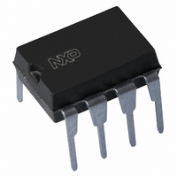
PCF8593P,112 NXP Semiconductors, PCF8593P,112 Datasheet - Page 28

PCF8593P,112
Manufacturer Part Number
PCF8593P,112
Description
IC CLOCK/CALENDAR LOW PWR 8-DIP
Manufacturer
NXP Semiconductors
Type
Clock/Calendar/NVSRAMr
Datasheet
1.PCF8593T1118.pdf
(35 pages)
Specifications of PCF8593P,112
Package / Case
8-DIP (0.300", 7.62mm)
Time Format
HH:MM:SS:hh (12/24 hr)
Date Format
YY-MM-DD-dd
Memory Size
8B
Interface
I²C, 2-Wire Serial
Voltage - Supply
1 V ~ 6 V
Operating Temperature
-40°C ~ 85°C
Mounting Type
Through Hole
Function
Clock/Calendar/Alarm/Timer Interrupt
Rtc Memory Size
8 Byte
Supply Voltage (max)
6 V
Supply Voltage (min)
1 V
Maximum Operating Temperature
+ 85 C
Minimum Operating Temperature
- 40 C
Mounting Style
Through Hole
Rtc Bus Interface
Serial (I2C)
Bus Type
Serial (I2C)
User Ram
8Byte
Package Type
PDIP
Operating Supply Voltage (max)
6V
Operating Temperature Classification
Industrial
Operating Temperature (max)
85C
Operating Temperature (min)
-40C
Pin Count
8
Mounting
Through Hole
Lead Free Status / RoHS Status
Lead free / RoHS Compliant
Lead Free Status / RoHS Status
Lead free / RoHS Compliant, Lead free / RoHS Compliant
Other names
568-1089-5
935151750112
PCF8593N
935151750112
PCF8593N
NXP Semiconductors
PCF8593
Product data sheet
13.4 Reflow soldering
Key characteristics in reflow soldering are:
Table 9.
Table 10.
Moisture sensitivity precautions, as indicated on the packing, must be respected at all
times.
Studies have shown that small packages reach higher temperatures during reflow
soldering, see
Package thickness (mm)
< 2.5
≥ 2.5
Package thickness (mm)
< 1.6
1.6 to 2.5
> 2.5
•
•
•
Lead-free versus SnPb soldering; note that a lead-free reflow process usually leads to
higher minimum peak temperatures (see
reducing the process window
Solder paste printing issues including smearing, release, and adjusting the process
window for a mix of large and small components on one board
Reflow temperature profile; this profile includes preheat, reflow (in which the board is
heated to the peak temperature) and cooling down. It is imperative that the peak
temperature is high enough for the solder to make reliable solder joints (a solder paste
characteristic). In addition, the peak temperature must be low enough that the
packages and/or boards are not damaged. The peak temperature of the package
depends on package thickness and volume and is classified in accordance with
Table 9
SnPb eutectic process (from J-STD-020C)
Lead-free process (from J-STD-020C)
and
Figure
All information provided in this document is subject to legal disclaimers.
10
26.
Rev. 04 — 6 October 2010
Package reflow temperature (°C)
Volume (mm
< 350
235
220
Package reflow temperature (°C)
Volume (mm
< 350
260
260
250
3
3
)
)
Figure
350 to 2000
260
250
245
26) than a SnPb process, thus
Low power clock and calendar
≥ 350
220
220
245
> 2000
260
245
PCF8593
© NXP B.V. 2010. All rights reserved.
28 of 35


