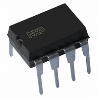
PCF8593P,112 NXP Semiconductors, PCF8593P,112 Datasheet - Page 12

PCF8593P,112
Manufacturer Part Number
PCF8593P,112
Description
IC CLOCK/CALENDAR LOW PWR 8-DIP
Manufacturer
NXP Semiconductors
Type
Clock/Calendar/NVSRAMr
Datasheet
1.PCF8593T1118.pdf
(35 pages)
Specifications of PCF8593P,112
Package / Case
8-DIP (0.300", 7.62mm)
Time Format
HH:MM:SS:hh (12/24 hr)
Date Format
YY-MM-DD-dd
Memory Size
8B
Interface
I²C, 2-Wire Serial
Voltage - Supply
1 V ~ 6 V
Operating Temperature
-40°C ~ 85°C
Mounting Type
Through Hole
Function
Clock/Calendar/Alarm/Timer Interrupt
Rtc Memory Size
8 Byte
Supply Voltage (max)
6 V
Supply Voltage (min)
1 V
Maximum Operating Temperature
+ 85 C
Minimum Operating Temperature
- 40 C
Mounting Style
Through Hole
Rtc Bus Interface
Serial (I2C)
Bus Type
Serial (I2C)
User Ram
8Byte
Package Type
PDIP
Operating Supply Voltage (max)
6V
Operating Temperature Classification
Industrial
Operating Temperature (max)
85C
Operating Temperature (min)
-40C
Pin Count
8
Mounting
Through Hole
Lead Free Status / RoHS Status
Lead free / RoHS Compliant
Lead Free Status / RoHS Status
Lead free / RoHS Compliant, Lead free / RoHS Compliant
Other names
568-1089-5
935151750112
PCF8593N
935151750112
PCF8593N
NXP Semiconductors
PCF8593
Product data sheet
7.10 Oscillator and divider
7.9 Interrupt control
this mode, the timer (location 07h) increments once for every one, one hundred, ten
thousand, or 1 million events, depending on the value programmed in bits 0, 1 and 2 of
the alarm control register. In all other events, the timer functions are as in the clock mode.
The conditions for activating the output INT (active LOW) are determined by appropriate
programming of the alarm control register. These conditions are clock alarm, timer alarm,
timer overflow, and event counter alarm. An interrupt occurs when the alarm flag or the
timer flag is set, and the corresponding interrupt is enabled. In all events, the interrupt is
cleared only by software resetting of the flag which initiated the interrupt.
In the clock mode, if the alarm enable is not activated (alarm enable bit of the control and
status register is logic 0), the interrupt output toggles at 1 Hz with a 50 % duty cycle (may
be used for calibration). The OFF voltage of the interrupt output may exceed the supply
voltage, up to a maximum of 6.0 V. A logic diagram of the interrupt output is shown in
Figure
A 32.768 kHz quartz crystal has to be connected to OSCI and OSCO. A trimmer capacitor
between OSCI and V
signal is derived from the quartz oscillator for the clock counters.
Fig 12. Alarm control register, event counter mode
11.
MSB
7
All information provided in this document is subject to legal disclaimers.
013aaa376
6
DD
Rev. 04 — 6 October 2010
is used for tuning the oscillator (see
5
4
3
2
1
LSB
0
clock alarm function:
00
01
10
11
memory location 08h
reset state: 0000 0000
000
001
010
011
100
101
110
111
timer interrupt enable:
0
1
timer function:
0
1
timer alarm enable:
0
1
alarm interrupt enable:
Low power clock and calendar
Section
no event alarm
event alarm
not allowed
not allowed
no timer alarm
timer alarm
no timer
units
100
10 000
1 000 000
not allowed
not allowed
test mode, all counters
in parallel
timer flag, no interrupt
timer flag, interrupt
alarm flag, no interrupt
alarm flag, interrupt
11.1). A 100 Hz clock
PCF8593
© NXP B.V. 2010. All rights reserved.
12 of 35


