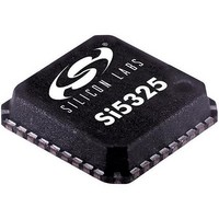
SI5325C-C-GM Silicon Laboratories Inc, SI5325C-C-GM Datasheet - Page 4

SI5325C-C-GM
Manufacturer Part Number
SI5325C-C-GM
Description
IC UP-PROG CLK MULTIPLIER 36-QFN
Manufacturer
Silicon Laboratories Inc
Type
Clock Multiplierr
Datasheet
1.SI5325C-C-GM.pdf
(52 pages)
Specifications of SI5325C-C-GM
Number Of Circuits
1
Package / Case
36-QFN
Pll
Yes
Input
Clock
Output
CML, CMOS, LVDS, LVPECL
Ratio - Input:output
2:2
Differential - Input:output
Yes/Yes
Frequency - Max
346MHz
Divider/multiplier
Yes/Yes
Voltage - Supply
1.71 V ~ 3.63 V
Operating Temperature
-40°C ~ 85°C
Mounting Type
Surface Mount
Frequency-max
346MHz
Maximum Input Frequency
710 MHz
Minimum Input Frequency
10 MHz
Output Frequency Range
10 MHz to 346 MHz
Supply Voltage (max)
3.63 V
Supply Voltage (min)
1.71 V
Maximum Operating Temperature
+ 85 C
Minimum Operating Temperature
- 40 C
Mounting Style
SMD/SMT
Operating Supply Voltage
1.8 V, 2.5 V, 3.3 V
Lead Free Status / RoHS Status
Lead free / RoHS Compliant
Available stocks
Company
Part Number
Manufacturer
Quantity
Price
Part Number:
SI5325C-C-GM
Manufacturer:
SILICONLABS/芯科
Quantity:
20 000
Si5325
Table 1. Performance Specifications
(V
4
Temperature Range
Supply Voltage
Supply Current
Input Clock Frequency
(CKIN1, CKIN2)
Output Clock Frequency
(CKOUT1, CKOUT2)
Input Clocks (CKIN1, CKIN2)
Input Voltage Level Limits
Differential Voltage Swing
Common Mode Voltage
Rise/Fall Time
(Minimum Pulse Width)
Output Clocks (CKOUT1, CKOUT2)
Common Mode
Differential Output Swing
Single Ended Output
Swing
Rise/Fall Time
Duty Cycle Uncertainty
Note: For a more comprehensive listing of device specifications, please consult the Silicon Laboratories Any-Frequency
Duty Cycle
DD
= 1.8 ±5%, 2.5 ±10%, or 3.3 V ±10%, T
Precision Clock Family Reference Manual. This document can be downloaded from
Documentation)
Parameter
.
CKN
CKN
CKN
CKO
Symbol
CKN
CKN
CKO
CK
V
CK
V
V
V
I
OCM
T
DD
DD
OD
SE
A
OF
VCM
DPP
TRF
TRF
VIN
F
DC
DC
ers. Consult Silicon Laboratories
for a given input frequency/clock
multiplication ratio combination.
Input frequency and clock multi-
A
programming device PLL divid-
configuration software DSPLL-
determine PLL divider settings
Line-to-Line Measured at 50%
sim at
plication ratio determined by
= –40 to 85 ºC)
(click on Documentation) to
Both CKOUTs enabled
Both CKOUTs enabled
LVPECL format output
CMOS format output
Whichever is smaller
f
CKOUT2 disabled
CKOUT2 disabled
OUT
f
Differential 100
Preliminary Rev. 0.4
OUT
www.silabs.com/timing
Test Condition
Disable Mode
2.5 V ±10%
3.3 V ±10%
100 load
1.8 V ±5%
line-to-line
= 622.08 MHz
LVPECL
20–80%
20–80%
= 19.44 MHz
LVPECL
point
V
DD
1213
2.97
2.25
1.71
.002
0.25
Min
–40
970
–40
0.9
1.0
1.1
1.1
0.5
10
40
—
—
—
—
—
—
– 1.42
0
2
www.silabs.com/timing
Typ
251
217
204
194
165
230
3.3
2.5
1.8
25
—
—
—
—
—
—
—
—
—
—
—
—
—
—
—
—
V
DD
1134
1400
Max
3.63
2.75
1.89
1.95
0.93
V
279
243
234
220
710
945
350
1.4
1.7
1.9
85
—
11
60
40
—
—
– 1.25
DD
(click on
Unit
MHz
MHz
V
mA
mA
mA
mA
mA
ºC
ns
ns
ps
ps
%
V
V
V
V
V
V
V
V
V
V
PP


