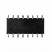
FS6370-01G-XTD ON Semiconductor, FS6370-01G-XTD Datasheet - Page 22

FS6370-01G-XTD
Manufacturer Part Number
FS6370-01G-XTD
Description
IC CLOCK GEN 3-PLL EEPROM 16SOIC
Manufacturer
ON Semiconductor
Type
PLL Clock Generatorr
Datasheet
1.FS6370-01G-XTD.pdf
(28 pages)
Specifications of FS6370-01G-XTD
Pll
Yes
Input
Crystal
Output
CMOS
Number Of Circuits
1
Ratio - Input:output
1:4
Differential - Input:output
No/No
Frequency - Max
230MHz
Divider/multiplier
Yes/No
Voltage - Supply
3 V ~ 5.5 V
Operating Temperature
0°C ~ 70°C
Mounting Type
Surface Mount
Package / Case
16-SOIC (3.9mm Width)
Frequency-max
230MHz
Mounting Style
SMD/SMT
Max Input Freq
230 MHz
Max Output Freq
27 MHz
Number Of Outputs
1
Operating Supply Voltage
5 V to 3.3 V
Operating Temperature Range
0 C to + 70 C
Supply Current
43 mA
Lead Free Status / RoHS Status
Lead free / RoHS Compliant
Other names
766-1025
Available stocks
Company
Part Number
Manufacturer
Quantity
Price
Company:
Part Number:
FS6370-01G-XTD
Manufacturer:
ON Semiconductor
Quantity:
38
FS6370
Table 13: AC Timing Specifications (Continued)
Unless otherwise stated, V
are not currently production tested to any specific limits. Min. and Max. characterization data are ± 3s from typical.
Table 14: Serial Interface Timing Specifications
Parameter
Clock Output (PLL C clock via CLK_C pin)
Clock Output (Crystal Oscillator via CLK_D pin)
Duty Cycle*
Jitter, Long Term (σ
Jitter, Period (peak-peak)*
Duty Cycle*
Jitter, Long Term (σ
Jitter, Period (peak-peak)*
Parameter
Clock frequency
Bus free time between STOP and START
Set up time, START (repeated)
Hold time, START
Set up time, data input
Hold time, data input
Output data valid from clock
Rise time, data and clock
Fall time, data and clock
High time, clock
Low time, clock
Set up time, STOP
DD
= 5.0V ± 10%, no load on any output, and ambient temperature range T
y
y
(τ))*
(τ))*
T
T
t
t
j(ΔP)
j(ΔP)
j(LT)
j(LT)
Symbol
Ratio of pulse width (as measured from rising edge to next falling
edge at 2.5V) to one clock period
On rising edges 500µs apart at 2.5V relative to an ideal clock,
C
active
On rising edges 500µs apart at 2.5V relative to an ideal clock,
C
active (A=50MHz, B=60MHz, D=14.318MHz)
From rising edge to the next rising edge at 2.5V, C
f
From rising edge to the next rising edge at 2.5V, C
f
(A=50MHz, B=60MHz, D=14.318MHz)
Ratio of pulse width (as measured from rising edge to next falling
edge at 2.5V) to one clock period
On rising edges 500µs apart at 2.5V relative to an ideal clock,
C
active
From rising edge to the next rising edge at 2.5V, C
f
C=40MHz)
From rising edge to the next rising edge at 2.5V, C
f
From rising edge to the next rising edge at 2.5V, C
f
C=40MHz)
XIN
XIN
XIN
XIN
XIN
L
L
L
=15pF, f
=15pF, f
=15pF, f
=14.318MHz, N
=14.318MHz, N
=14.318MHz, all other PLLs active (A=50MHz, B=60MHz,
=14.318MHz, no other PLLs active
=14.318MHz, all other PLLs active (A=50MHz, B=60MHz,
Symbol
t
t
t
t
t
su:STA
hd:STA
su:DAT
hd:DAT
su:STO
f
t
t
t
SCL
BUF
t
t
t
AA
LO
Conditions/Description
HI
R
F
XIN
XIN
XIN
Rev. 3 | Page 22 of 28 | www.onsemi.com
=14.318MHz, N
=14.318MHz, N
=14.318MHz, N
F
F
=220, N
=220, N
Conditions/Description
SCL
SDA
SDA
Minimum delay to bridge undefined region of the falling
edge of SCL to avoid unintended START or STOP
SDA, SCL
SDA, SCL
SCL
SCL
R
R
=63, N
=63, N
F
F
F
=220, N
=220, N
=220, N
Px
Px
=50, no other PLLs active
=50, all other PLLs active
R
R
R
A
=63, N
=63, N
=63, N
= 0°C to 70°C. Parameters denoted with an asterisk ( * ) represent nominal characterization data and
Px
Px
Px
=50, no other PLLs
=50, all other PLLs
=50, no other PLLs
L
L
L
L
L
=15pF,
=15pF,
=15pF,
=15pF,
=15pF,
14.318
14.318
14.318
14.318
14.318
Clock
(MHz)
100
100
100
40
40
Min.
250
4.7
4.7
4.0
4.0
4.7
4.0
Min.
0
0
45
45
Typ.
105
120
440
450
45
20
40
90
Max.
1000
100
300
3.5
Max.
55
55
Units
kHz
μs
μs
μs
μs
μs
μs
μs
μs
ns
ns
ns
Units
ps
ps
ps
ps
%
%


