FS6370-01G-XTD ON Semiconductor, FS6370-01G-XTD Datasheet - Page 21

FS6370-01G-XTD
Manufacturer Part Number
FS6370-01G-XTD
Description
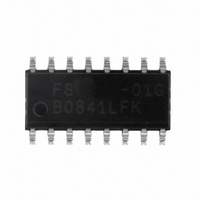
IC CLOCK GEN 3-PLL EEPROM 16SOIC
Manufacturer
ON Semiconductor
Type
PLL Clock Generatorr
Datasheet
1.FS6370-01G-XTD.pdf
(28 pages)
Specifications of FS6370-01G-XTD
Pll
Yes
Input
Crystal
Output
CMOS
Number Of Circuits
1
Ratio - Input:output
1:4
Differential - Input:output
No/No
Frequency - Max
230MHz
Divider/multiplier
Yes/No
Voltage - Supply
3 V ~ 5.5 V
Operating Temperature
0°C ~ 70°C
Mounting Type
Surface Mount
Package / Case
16-SOIC (3.9mm Width)
Frequency-max
230MHz
Mounting Style
SMD/SMT
Max Input Freq
230 MHz
Max Output Freq
27 MHz
Number Of Outputs
1
Operating Supply Voltage
5 V to 3.3 V
Operating Temperature Range
0 C to + 70 C
Supply Current
43 mA
Lead Free Status / RoHS Status
Lead free / RoHS Compliant
Other names
766-1025
Available stocks
Company
Part Number
Manufacturer
Quantity
Price
Company:
Part Number:
FS6370-01G-XTD
Manufacturer:
ON Semiconductor
Quantity:
38
FS6370
Table 13: AC Timing Specifications
Parameter
Overall
Divider Modulus
Clock Output (PLL A clock via CLK_A pin)
Clock Output (PLL B clock via CLK_B pin)
EEPROM Write Cycle Time
Output Frequency *
VCO Frequency *
VCO Gain *
Loop Filter Time Constant *
Rise Time *
Fall Time *
Tristate Enable Delay *
Tristate Disable Delay *
Clock Stabilization Time *
Feedback Divider
Reference Divider
Post Divider
Duty Cycle *
Jitter, Long Term (σ
Jitter, Period (peak-peak)
*
Duty Cycle *
Jitter, Long Term (σ
Jitter, Period (peak-peak)
*
y
y
(τ)) *
(τ)) *
T
T
N
N
N
t
t
j(ΔP)
j(ΔP)
j(LT)
j(LT)
R
F
P
Symbol
t
t
PZL,
PZL,
A
f
t
T
VCO
STB
f
VCO
t
t
wc
O
r
f
t
t
PZH
PZH
See also Error! Reference source not found.
See also Error! Reference source not found.
Ratio of pulse width (as measured from rising edge to next falling
edge at 2.5V) to one clock period
On rising edges 500µs apart at 2.5V relative to an ideal clock,
CL=15pF, fXIN=14.318MHz, NF=220, NR=63, NPX=50, no other
PLLs active
On rising edges 500µs apart at 2.5V relative to an ideal clock,
CL=15pF, =14.318MHz, NF=220, NR=63, NPX=50, all other
PLLs active (B=60MHz, C=40MHz, D=14.318MHz)
From rising edge to the next rising edge at 2.5V, CL=15pF,
fXIN=14.318MHz, NF=220, NR=63, NPX=50, no other PLLs
active
From rising edge to the next rising edge at 2.5V, CL=15pF,
fXIN=14.318MHz, NF=220, NR=63, NPX=50, all other PLLs
active (B=60MHz, C=40MHz, D=14.318MHz)
Ratio of pulse width (as measured from rising edge to next falling
edge at 2.5V) to one clock period
On rising edges 500µs apart at 2.5V relative to an ideal clock,
CL=15pF, fXIN=14.318MHz, NF=220, NR=63, NPX=50, no other
PLLs active
On rising edges 500µs apart at 2.5V relative to an ideal clock,
CL=15pF, =14.318MHz, NF=220, NR=63, NPX=50, all other
PLLs active (A=50MHz, C=40MHz, D=14.318MHz)
From rising edge to the next rising edge at 2.5V, CL=15pF,
fXIN=14.318MHz, NF=220, NR=63, NPX=50, no other PLLs
active
From rising edge to the next rising edge at 2.5V, CL=15pF,
fXIN=14.318MHz, NF=220, NR=63, NPX=50, all other PLLs
active (A=50MHz, C=40MHz, D=14.318MHz)
Conditions/Description
V
V
V
V
LFTC bit = 0
LFTC bit = 1
V
V
V
V
Output active from power-up, RUN mode via PD pin
After last register is written, register program mode
DD
DD
O
O
O
O
DD
DD
Rev. 3 | Page 21 of 28 | www.onsemi.com
= 0.5 V to 4.5 V; C
= 0.3 V to 3.0 V; C
= 4.5 V to 0.5 V; C
= 3.0 V to 0.3 V; C
= 5.5 V
= 3.6 V
= 5.5 V
= 3.6 V
L
L
L
L
= 15pF
= 15pF
= 15pF
= 15pF
Clock
(MHz)
100
100
100
100
100
100
50
50
60
60
Min.
0.8
0.8
40
40
45
45
1
1
8
1
1
Typ.
400
100
165
110
390
120
400
2.0
2.1
1.8
1.9
20
45
45
75
7
Max.
2047
150
100
230
170
255
50
55
55
4
8
8
1
MHz/V
Units
MHz
MHz
ms
ms
μs
ns
ns
ns
ns
μs
ps
ps
ps
ps
%
%


