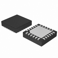
NB6L295MNTXG ON Semiconductor, NB6L295MNTXG Datasheet - Page 9

NB6L295MNTXG
Manufacturer Part Number
NB6L295MNTXG
Description
IC CLOCK/DATA DELAY 2CH 24-QFN
Manufacturer
ON Semiconductor
Type
Programmable Delay Chipr
Datasheet
1.NB6L295MNTXG.pdf
(14 pages)
Specifications of NB6L295MNTXG
Input
CML, LVDS, LVPECL
Output
CML
Frequency - Max
1.5GHz
Voltage - Supply
2.4 V ~ 3.6 V
Operating Temperature
-40°C ~ 85°C
Mounting Type
Surface Mount
Package / Case
24-TFQFN Exposed Pad
Frequency-max
1.5GHz
Lead Free Status / RoHS Status
Lead free / RoHS Compliant
Available stocks
Company
Part Number
Manufacturer
Quantity
Price
Company:
Part Number:
NB6L295MNTXG
Manufacturer:
ON Semiconductor
Quantity:
40
Part Number:
NB6L295MNTXG
Manufacturer:
ON/安森美
Quantity:
20 000
Serial Data Interface Loading
using the SCLK input pin and latching the data with the SLOAD input pin. The 11−bit SHIFT REGISTER shifts once per rising
edge of the SCLK input. The serial input SDIN must meet setup and hold timing as specified in the AC Characteristics section
of this document for each bit and clock pulse. The SLOAD line loads the value of the shift register on a LOW−to−HIGH edge
transition (transparent state) into a data Latch register and latches the data with a subsequent HIGH−to−LOW edge transition.
Further changes in SDIN or SCLK are not recognized by the latched register. The internal multiplexer states are set by the PSEL
and MSEL bits in the SHIFT register. Figure 6 shows the timing diagram of a typical load sequence. Input EN should be LOW
(enabled) prior to SDI programming, then pulled HIGH (disabled) during programming. After programming, the EN should
be returned LOW (enabled) for functional delay operation.
Loading the device through the 3 input Serial Data Interface (SDI) is accomplished by sending data into the SDIN pin by
EN
t
SLOAD
s
SCLK
SDIN to
SDIN
SCLK
Figure 7. Serial Data Interface, Shift Register, Data Latch, Programmable Delay Channels
SLOAD
LSB
PSEL
C0
MSEL
C1
t
SDATA
h
SCLK
SDIN to SCLK
PD0 Latch
D0
PD0 Delay
C2
D1
C3
Figure 8. SDI Timing Diagram
11−Bit Shift Register
MSEL
D2
0
http://onsemi.com
C4
Q0/Q0
D3
C5
9
D4
1
C6
D5
C7
PD1 Delay
t
s
PD1 Latch
SCLK to SLOAD
D6
C8
D7
C9
Q1/Q1
MSB
D8
C10
t
pwmin


