NB6L295MNTXG ON Semiconductor, NB6L295MNTXG Datasheet

IC CLOCK/DATA DELAY 2CH 24-QFN

NB6L295MNTXG

Manufacturer Part Number
NB6L295MNTXG
Description
IC CLOCK/DATA DELAY 2CH 24-QFN
Manufacturer
ON Semiconductor
Type
Programmable Delay Chipr
Datasheet

Specifications of NB6L295MNTXG

Input
CML, LVDS, LVPECL
Output
CML
Frequency - Max
1.5GHz
Voltage - Supply
2.4 V ~ 3.6 V
Operating Temperature
-40°C ~ 85°C
Mounting Type
Surface Mount
Package / Case
24-TFQFN Exposed Pad
Frequency-max
1.5GHz
Lead Free Status / RoHS Status
Lead free / RoHS Compliant

Available stocks

Company
Part Number
Manufacturer
Quantity
Price
Part Number:
NB6L295MNTXG
Manufacturer:
ON Semiconductor
Quantity:
40
Part Number:
NB6L295MNTXG
Manufacturer:
ON/安森美
Quantity:
20 000
NB6L295
2.5V / 3.3V Dual Channel
Programmable Clock/Data
Delay with Differential
LVPECL Outputs
Multi−Level Inputs w/ Internal Termination
designed primarily for Clock or Data de−skewing and timing
adjustment. The NB6L295 is versatile in that two individual variable
delay channels, PD0 and PD1, can be configured in one of two
operating modes, a Dual Delay or an Extended Delay.
section which is designed using a matrix of gates and a chain of
multiplexers. There is a fixed minimum delay of 3.2 ns per channel.
plus PD1 and is accomplished with the Serial Data Interface MSEL bit
set High. This will internally cascade the output of PD0 into the input
of PD1. Therefore, the Extended Delay path starts at the IN0/IN0
inputs, flows through PD0, cascades to the PD1 and outputs through
Q1/Q1. There is a fixed minimum delay of 6 ns for the Extended
Delay Mode.
channel via a 3−pin Serial Data Interface, described in the application
section. The digitally selectable delay has an increment resolution of
typically 11 ps with a net programmable delay range of either 0 ns to
6 ns per channel in Dual Delay Mode; or from 0 ns to 11.2 ns for the
Extended Delay Mode.
LVPECL, LVDS or CML logic levels; or by single ended LVPECL,
LVCMOS or LVTTL. A single enable pin is available to control both
inputs. The SDI input pins are controlled by LVCMOS or LVTTL
level signals. The NB6L295 LVPECL output contains temperature
compensation circuitry. This device is offered in a 4 mm x 4 mm
24−pin QFN Pb−free package. The NB6L295 is a member of the
ECLinPS MAX™ family of high performance products.
*For additional information on our Pb−Free strategy and soldering details, please
© Semiconductor Components Industries, LLC, 2010
January, 2010 − Rev. 3
download the ON Semiconductor Soldering and Mounting Techniques
Reference Manual, SOLDERRM/D.
The NB6L295 is a Dual Channel Programmable Delay Chip
In the Dual Delay Mode, each channel has a programmable delay
The Extended Delay Mode amounts to the additive delay of PD0
The required delay is accomplished by programming each delay
The Multi−Level Inputs can be driven directly by differential
Input Clock Frequency > 1.5 GHz with 550 mV
V
Input Data Rate > 2.5 Gb/s
Programmable Delay Range: 0 ns to 6 ns per Delay
Channel
Programmable Delay Range: 0 ns to 11.2 ns for
Extended Delay Mode
Total Delay Range: 3.2 ns to 8.8 ns per Delay Channel
Total Delay Range: 6 ns to 17 ns in Extended Delay
Mode
Monotonic Delay: 11 ps Increments in 511 Steps
Linearity $20 ps, Maximum
100 ps Typical Rise and Fall Times
OUTPP
1
3 ps Typical Clock Jitter, RMS
20 ps Pk−Pk Typical Data Dependent Jitter
LVPECL, CML or LVDS Differential Input Compatible
LVPECL, LVCMOS, LVTTL Single−Ended Input
Compatible
3−Wire Serial Interface
Operating Range: V
LVPECL Output Level; 780 mV Peak−to−Peak, Typical
Internal 50 W Input Termination Provided
−40°C to 85°C Ambient Operating Temperature
24−Pin QFN, 4 mm x 4 mm
These are Pb−Free Devices*
See detailed ordering and shipping information in the package
dimensions section on page 13 of this data sheet.
24
*For additional marking information, refer to
Application Note AND8002/D.
A
L
Y
W
G
(Note: Microdot may be in either location)
1
ORDERING INFORMATION
CC
= Assembly Location
= Wafer Lot
= Year
= Work Week
= Pb−Free Package
http://onsemi.com
= 2.375 V to 3.6 V
MN SUFFIX
CASE 485L
QFN−24
Publication Order Number:
1
DIAGRAM*
MARKING
24
ALYWG
NB6L295/D
NB6L
295
G

Related parts for NB6L295MNTXG

NB6L295MNTXG Summary of contents

Page 1

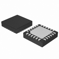
... Linearity $20 ps, Maximum • 100 ps Typical Rise and Fall Times *For additional information on our Pb−Free strategy and soldering details, please download the ON Semiconductor Soldering and Mounting Techniques Reference Manual, SOLDERRM/D. © Semiconductor Components Industries, LLC, 2010 January, 2010 − Rev. 3 http://onsemi.com QFN− ...

Page 2

Figure 1. Simplified Functional Block Diagram http://onsemi.com 2 ...

Page 3

VCC EN SLOAD SDIN SCLK VCC Table 1. PIN DESCRIPTION Pin Name I/O 1 VCC Power Supply 2 EN LVCMOS/LVTTL Input 3 SLOAD LVCMOS/LVTTL Input 4 SDIN LVCMOS/LVTTL Input 5 SCLK LVCMOS/LVTTL Input 6 VCC Power Supply 7 VT1 8 ...

Page 4

Table 2. ATTRIBUTES Input Default State Resistors ESD Protection Moisture Sensitivity (Note 3) Flammability Rating Transistor Count Meets or exceeds JEDEC Spec EIA/JESD78 IC Latchup Test 3. For additional information, see Application Note AND8003/D. Table 3. MAXIMUM RATINGS Symbol Parameter ...

Page 5

Table 4. DC CHARACTERISTICS, MULTI−LEVEL INPUTS +85°C Symbol Characteristic POWER SUPPLY CURRENT I Power Supply Current (Inputs and I ) CC0 CC1 LVPECL OUTPUTS (Notes 5 and 6, Figure 21) V Output HIGH Voltage OH V ...

Page 6

Table 5. AC CHARACTERISTICS V Symbol f Serial Clock Input Frequency, 50% Duty Cycle SCLK V Output Voltage Amplitude (@ V OUTPP f Maximum Data Rate (Note 14) DATA t Programmable Delay Range (@ 50 MHz) Range Dual Mode Extended ...

Page 7

Table 6. AC CHARACTERISTICS V Symbol Characteristic t , Propagation Delay (@ 50 MHz) PLH t Dual Mode IN0/IN0 to Q0/Q0 or IN1/IN1 to Q1/Q1 PHL Extended Mode Dt Step Delay (Selected D Bit HIGH All Others LOW) NOTE: Device ...

Page 8

Serial Data Interface Programming The NB6L295 is programmed by loading the 11−Bit SHIFT REGISTER using the SCLK, SDATA and SLOAD inputs. The 11 SDATA bits are 1 PSEL bit, 1 MSEL bit and 9 delay value data bitsD[8:0]. A separate ...

Page 9

PD0 Delay SLOAD PD0 Latch SDATA SCLK Figure 7. Serial Data Interface, Shift Register, Data Latch, Programmable Delay Channels Serial Data Interface Loading Loading the device through the 3 input Serial Data Interface (SDI) is accomplished by sending data into ...

Page 10

Table 8 shows theoretical values of delay capabilities in both the Dual Delay Mode and in the Extended Delay Modes of operation. Table 8. EXAMPLES OF THEORETICAL DELAY VALUES FOR PD0 AND PD1 IN DUAL MODE INPUTS: IN0/IN0, IN1/IN1, OUTPUTS: ...

Page 11

INx INx V th Figure 10. Differential Input Driven Single−Ended INx INx Figure 12. Differential Inputs Driven Differentially IHD(MAX) V ILD(MAX) V IHD CMR ID V ILD ...

Page 12

V CC INx NB6L295 LVPECL T Driver INx − 2 ...

Page 13

... Figure 22. Output Voltage Amplitude (V Output Frequency at Ambient Temperature (Typical) ORDERING INFORMATION Device NB6L295MNG NB6L295MNTXG †For information on tape and reel specifications, including part orientation and tape sizes, please refer to our Tape and Reel Packaging Specifications Brochure, BRD8011/ ...

Page 14

... American Technical Support: 800−282−9855 Toll Free USA/Canada Japan: ON Semiconductor, Japan Customer Focus Center 2−9−1 Kamimeguro, Meguro−ku, Tokyo, Japan 153−0051 Phone: 81−3−5773−3850 http://onsemi.com 14 NOTES: 1. DIMENSIONING AND TOLERANCING PER ASME Y14.5M, 1994. 2. CONTROLLING DIMENSION: MILLIMETERS. ...

Related keywords