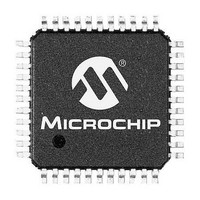
PIC24FV32KA304-I/PT Microchip Technology, PIC24FV32KA304-I/PT Datasheet - Page 243

PIC24FV32KA304-I/PT
Manufacturer Part Number
PIC24FV32KA304-I/PT
Description
MCU 32KB FLASH 2KB RAM 44-TQFP
Manufacturer
Microchip Technology
Specifications of PIC24FV32KA304-I/PT
Processor Series
PIC24FV
Core
PIC
Data Bus Width
16 bit
Program Memory Type
Flash
Program Memory Size
32 KB
Data Ram Size
2 KB
Maximum Operating Temperature
+ 85 C
Mounting Style
SMD/SMT
Package / Case
TQFP-44
Development Tools By Supplier
MPLAB IDE Software
Minimum Operating Temperature
- 40 C
Lead Free Status / Rohs Status
Lead free / RoHS Compliant
Available stocks
Company
Part Number
Manufacturer
Quantity
Price
Company:
Part Number:
PIC24FV32KA304-I/PT
Manufacturer:
VISHAY
Quantity:
12 000
Company:
Part Number:
PIC24FV32KA304-I/PT
Manufacturer:
Microchip Technology
Quantity:
10 000
- Current page: 243 of 320
- Download datasheet (3Mb)
REGISTER 26-6:
2011 Microchip Technology Inc.
bit 7
Legend:
R = Readable bit
-n = Value at POR
bit 7
bit 6-5
bit 4
bit 3
bit 2
bit 1-0
Note 1:
MCLRE
R/P-1
2:
3:
(2)
This setting only applies to the “FV” devices. This bit is reserved and should be maintained as ‘1’ on “F”
devices.
The MCLRE fuse can only be changed when using the V
user from accidentally locking out the device from the low-voltage test entry.
Refer to
MCLRE: MCLR Pin Enable bit
1 = MCLR pin is enabled; RA5 input pin is disabled
0 = RA5 input pin is enabled; MCLR is disabled
BORV<1:0>: Brown-out Reset Enable bits
11 = Brown-out Reset set to lowest voltage
10 = Brown-out Reset
01 = Brown-out Reset set to highest voltage
00 = Downside protection on POR is enabled – “zero-power” is selected
I2C1SEL: Alternate I2C1 Pin Mapping bit
1 = Default location for SCL1/SDA1 pins
0 = Alternate location for SCL1/SDA1 pins
PWRTEN: Power-up Timer Enable bit
1 = PWRT is enabled
0 = PWRT is disabled
LVRCFG: Low-Voltage Regulator Configuration bit
1 = Low-voltage regulator is not available
0 = Low-voltage regulator is available and controlled by the LVREN bit (RCON<12>) during Sleep
BOREN<1:0>: Brown-out Reset Enable bits
11 = Brown-out Reset is enabled in hardware; SBOREN bit is disabled
10 = Brown-out Reset is enabled only while device is active and disabled in Sleep; SBOREN bit is disabled
01 = Brown-out Reset is controlled with the SBOREN bit setting
00 = Brown-out Reset is disabled in hardware; SBOREN bit is disabled
BORV1
R/P-1
Section 29.0 “Electrical Characteristics”
FPOR: RESET CONFIGURATION REGISTER
(3)
P = Programmable bit
‘1’ = Bit is set
BORV0
R/P-1
(3)
(2)
I2C1SEL
R/P-1
PIC24FV32KA304 FAMILY
(1)
(1)
(3)
U = Unimplemented bit, read as ‘0’
‘0’ = Bit is cleared
PWRTEN
R/P-1
for BOR voltages.
(1)
PP
-Based ICSP™ mode entry. This prevents a
LVRCFG
R/P-1
(1)
x = Bit is unknown
BOREN1
R/P-1
DS39995B-page 243
BOREN0
R/P-1
bit 0
Related parts for PIC24FV32KA304-I/PT
Image
Part Number
Description
Manufacturer
Datasheet
Request
R

Part Number:
Description:
Manufacturer:
Microchip Technology Inc.
Datasheet:

Part Number:
Description:
Manufacturer:
Microchip Technology Inc.
Datasheet:

Part Number:
Description:
Manufacturer:
Microchip Technology Inc.
Datasheet:

Part Number:
Description:
Manufacturer:
Microchip Technology Inc.
Datasheet:

Part Number:
Description:
Manufacturer:
Microchip Technology Inc.
Datasheet:

Part Number:
Description:
Manufacturer:
Microchip Technology Inc.
Datasheet:

Part Number:
Description:
Manufacturer:
Microchip Technology Inc.
Datasheet:

Part Number:
Description:
Manufacturer:
Microchip Technology Inc.
Datasheet:


