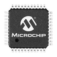
PIC24FV32KA304-I/PT Microchip Technology, PIC24FV32KA304-I/PT Datasheet - Page 239

PIC24FV32KA304-I/PT
Manufacturer Part Number
PIC24FV32KA304-I/PT
Description
MCU 32KB FLASH 2KB RAM 44-TQFP
Manufacturer
Microchip Technology
Specifications of PIC24FV32KA304-I/PT
Processor Series
PIC24FV
Core
PIC
Data Bus Width
16 bit
Program Memory Type
Flash
Program Memory Size
32 KB
Data Ram Size
2 KB
Maximum Operating Temperature
+ 85 C
Mounting Style
SMD/SMT
Package / Case
TQFP-44
Development Tools By Supplier
MPLAB IDE Software
Minimum Operating Temperature
- 40 C
Lead Free Status / Rohs Status
Lead free / RoHS Compliant
Available stocks
Company
Part Number
Manufacturer
Quantity
Price
Company:
Part Number:
PIC24FV32KA304-I/PT
Manufacturer:
VISHAY
Quantity:
12 000
Company:
Part Number:
PIC24FV32KA304-I/PT
Manufacturer:
Microchip Technology
Quantity:
10 000
- Current page: 239 of 320
- Download datasheet (3Mb)
26.0
PIC24FV32KA304 family devices include several
features intended to maximize application flexibility and
reliability, and minimize cost through elimination of
external components. These are:
• Flexible Configuration
• Watchdog Timer (WDT)
• Code Protection
• In-Circuit Serial Programming™ (ICSP™)
• In-Circuit Emulation
REGISTER 26-1:
2011 Microchip Technology Inc.
bit 7
Legend:
R = Readable bit
-n = Value at POR
bit 7-4
bit 3-1
bit 0
Note 1:
Note:
U-0
—
SPECIAL FEATURES
This selection should not be used in PIC24FV16KA3XX devices.
This data sheet summarizes the features
of this group of PIC24F devices. It is not
intended
reference source. For more information
on the Watchdog Timer, High-Level
Device Integration and Programming
Diagnostics, refer to the individual sec-
tions of the “PIC24F Family Reference
Manual” provided below:
• Section 9. “Watchdog Timer (WDT)”
• Section 36. “High-Level Integration
• Section 33. “Programming and
(DS39697)
with Programmable High/Low-
Voltage Detect (HLVD)” (DS39725)
Diagnostics” (DS39716)
Unimplemented: Read as ‘0’
BSS<2:0>: Boot Segment Program Flash Code Protection bits
111 = No boot program Flash segment
011 = Reserved
110 = Standard security, boot program Flash segment starts at 200h, ends at 000AFEh
010 = High-security boot program Flash segment starts at 200h, ends at 000AFEh
101 = Standard security, boot program Flash segment starts at 200h, ends at 0015FEh
001 = High-security, boot program Flash segment starts at 200h, ends at 0015FEh
100 = Standard security; boot program Flash segment starts at 200h, ends at 002BFEh
000 = High-security; boot program Flash segment starts at 200h, ends at 002BFEh
BWRP: Boot Segment Program Flash Write Protection bit
1 = Boot segment may be written
0 = Boot segment is write-protected
U-0
—
FBS: BOOT SEGMENT CONFIGURATION REGISTER
to
be
W = Writable bit
‘1’ = Bit is set
a
U-0
—
comprehensive
PIC24FV32KA304 FAMILY
U-0
—
U = Unimplemented bit, read as ‘0’
‘0’ = Bit is cleared
R/W-1
26.1
The Configuration bits can be programmed (read as ‘0’),
or left unprogrammed (read as ‘1’), to select various
device configurations. These bits are mapped starting at
program memory location, F80000h. A complete list is
provided in
various bit functions is provided in
Register
The address, F80000h, is beyond the user program
memory space. In fact, it belongs to the configuration
memory space (800000h-FFFFFFh), which can only be
accessed using table reads and table writes.
TABLE 26-1:
BSS2
FBS
FGS
FOSCSEL
FOSC
FWDT
FPOR
FICD
FDS
Configuration
Register
26-8.
Configuration Bits
Table
R/W-1
BSS1
CONFIGURATION REGISTERS
LOCATIONS
26-1. A detailed explanation of the
x = Bit is unknown
R/W-1
BSS0
Address
Register 26-1
F8000C
F8000A
F8000E
F80000
F80004
F80006
F80008
F80010
(1)
(1)
DS39995B-page 239
(1)
(1)
BWRP
R/W-1
through
bit 0
Related parts for PIC24FV32KA304-I/PT
Image
Part Number
Description
Manufacturer
Datasheet
Request
R

Part Number:
Description:
Manufacturer:
Microchip Technology Inc.
Datasheet:

Part Number:
Description:
Manufacturer:
Microchip Technology Inc.
Datasheet:

Part Number:
Description:
Manufacturer:
Microchip Technology Inc.
Datasheet:

Part Number:
Description:
Manufacturer:
Microchip Technology Inc.
Datasheet:

Part Number:
Description:
Manufacturer:
Microchip Technology Inc.
Datasheet:

Part Number:
Description:
Manufacturer:
Microchip Technology Inc.
Datasheet:

Part Number:
Description:
Manufacturer:
Microchip Technology Inc.
Datasheet:

Part Number:
Description:
Manufacturer:
Microchip Technology Inc.
Datasheet:


