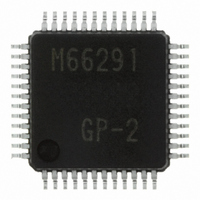
M66291GP#201 Renesas Electronics America, M66291GP#201 Datasheet - Page 7

M66291GP#201
Manufacturer Part Number
M66291GP#201
Description
IC USB CONTROLLER GEN-PUR 48LQFP
Manufacturer
Renesas Electronics America
Datasheet
1.M66291GP201.pdf
(126 pages)
Specifications of M66291GP#201
Package / Case
48-LQFP
Mounting Type
Surface Mount
Current - Supply
30mA
Voltage - Supply
3 V ~ 3.6 V
Operating Temperature
-20°C ~ 85°C
Interface
Serial
Controller Type
USB 2.0 Controller
Lead Free Status / RoHS Status
Not Compliant
Available stocks
Company
Part Number
Manufacturer
Quantity
Price
M 6 6 2 9 1 G P / H P
1.3 Pin Functions
R e v 1 . 0 1
Bus
interface
Interrupt
interface
DMA
interface
Item
2 0 0 4 . 1 1 . 0 1
D7~D0
D14/P6~
D8/P0
D15/A0
A6~A1
*CS
*LWR
*HWR/*BYTE Input
*RD
*INT0
(Note 1)
*INT1/*SOF
(Note 1)
*Dreq0
(Note 1)
*Dack0
(Note 1)
*Dreq1
(Note 1)
Pin name
p a g e 7 o f 1 2 2
Input/
Output
Input/
Output
Input/
Output
Input
Input
Input
Input
Output
Output
Output
Input
Output
Output
Input/
Data Bus
This is a data bus to access the register from the system bus.
Data Bus / Port Signal
P6 to P0 are used as port signals when selected to 8-bit bus interface.
D14 to D8 are used as data signals when selected to 16-bit bus interface.
D15 Signal / A0 Signal
A0 (LSB) is used as an address signal when selected to 8-bit bus interface.
D15 (MSB) is used as an data signal when selected to 16-bit bus interface.
Address Bus
This is an address bus to access the register from the system bus.
Chip Select
"L" level enables communication with the M66291.
Low-write Strobe
The lower data (D7 to D0) is written to the register at “L” level.
High-write Strobe / Bus Width Select
With the reset signal set to “H” level, the 8-bit bus interface is selected if this
pin is at “L” level. Further, if this pin is at “H” level, the 16-bit bus interface is
selected. When the 16-bit bus interface is selected, the upper data (D15 to
D8) is written to the register at “L” level.
Fix to “L” level when set to 8-bit bus interface.
Read Strobe
Data are read from registers at "L" level
Interrupt 0
Interrupts are requested to the system at "L" level.
Interrupt 1 / SOF Output
This pin is used as an interrupt 1 or as a SOF output pin to transmit USB SOF
signal according to register setting.
DMA Request 0
This pin is used to request DMA transfer to endpoint FIFO for DMA channel 0.
DMA Acknowledge 0
This pin enables access of FIFO by DMA transfer for DMA channel 0.
DMA Request 1
This pin is used to request DMA transfer to endpoint FIFO for DMA channel 1.
Function
Count
8
7
1
6
1
1
1
1
1
1
1
1
1
Pin


