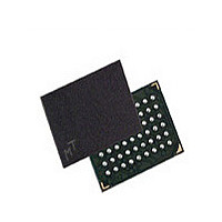
MT45W4MW16PCGA-70 L WT Micron Technology Inc, MT45W4MW16PCGA-70 L WT Datasheet - Page 18

MT45W4MW16PCGA-70 L WT
Manufacturer Part Number
MT45W4MW16PCGA-70 L WT
Description
Manufacturer
Micron Technology Inc
Datasheet
1.MT45W4MW16PCGA-70_L_WT.pdf
(23 pages)
Specifications of MT45W4MW16PCGA-70 L WT
Operating Temperature (max)
85C
Mounting
Surface Mount
Operating Temperature Classification
Commercial
Lead Free Status / RoHS Status
Compliant
Table 12:
PDF: 09005aef81f0698d / Source: 09005aef81f06935
64mb_asyncpage_cr1_0_p25z.fm - Rev. D 7/09 EN
Parameter
Address and ADV# LOW setup time
Address valid to end of WRITE
LB#/UB# select to end of WRITE
CE# HIGH time during WRITEs between subsequent async operations
Chip enable to end of WRITE
Data hold from WRITE time
Data WRITE setup time
Chip enable to Low-Z output
End WRITE to Low-Z output
WRITE cycle time
WRITE to DQ High-Z output
WRITE pulse width
WRITE pulse width HIGH
WRITE recovery time
Asynchronous WRITE Cycle Timing Requirements
Notes:
1. Low-Z to High-Z timings are tested with the circuit shown in Figure 15 on page 16. The
2. High-Z to Low-Z timings are tested with the circuit shown in Figure 15 on page 16. The Low-
3. WE# LOW time must be limited to
High-Z timings measure a 100mV transition from either V
Z timings measure a 100mV transition away from the High-Z (V
V
OH
or V
OL
.
64Mb: 4 Meg x 16 Async/Page CellularRAM 1.0
18
t
CEM (4µs).
Micron Technology, Inc., reserves the right to change products or specifications without notice.
Symbol
t
t
t
t
t
t
t
t
t
WHZ
t
WPH
t
t
t
CPH
AW
DW
t
OW
BW
CW
WC
WP
WR
DH
AS
LZ
Min
70
70
70
20
10
70
45
10
0
5
0
5
0
OH
70ns
or V
Timing Requirements
CC
©2005 Micron Technology, Inc. All rights reserved.
Max
OL
Q/2) level toward either
8
toward V
Unit
ns
ns
ns
ns
ns
ns
ns
ns
ns
ns
ns
ns
ns
ns
CC
Q/2.
Notes
2
2
1
3


